


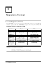
24
•
Operation Theorem
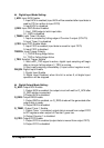
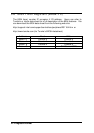
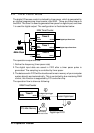
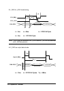
4.2 Timer Pacer Mode
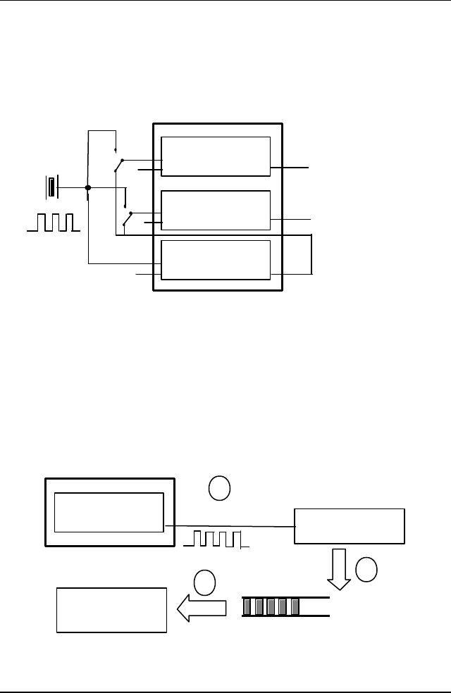
The digital I/O access control is clocked by timer pacer, which is generated by
an interval programming timer/counter chip 8254. There are three timers on
the 8254. The timer 0 is used to generate timer pacer for digital input, and timer
1 is used for digital output. The configuration is illustrated as below.
Timer 0
Timer 1
Timer 2
CLK0
GATE0
OUT0
CLK1
GATE1
CLK2
GATE2
OUT1
OUT2
8254 Timer/Counter
Digital Input Timer Pacer
Digital Output Timer Pacer
4MHz Clock
“H”
“H”
“H”
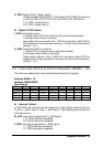
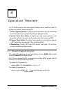
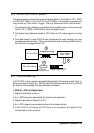
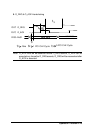
The operation sequences are:
1. Define the frequency (timer pacer rate)
2. The digital input data are saved in FIFO after a timer pacer pulse is
generated. The sampling is controlled by timer pacer.
3. The data saved in FIFO will be transferred to main memory of your computer
system directly and automatically. This is controlled by bus mastering DMA
control, this function is supported by PCI controller chip.
The operation flow is show as following:
Timer 0
CLK0
GATE0
OUT0
8254 Timer/Counter
To Digital Input Trigger
Latch Digital Input
Digital Input FIFO
Bus mastering
DMA data Transfer
PC's Main Memory
1
2
3