


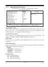

28
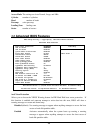
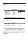
CAS Latency
When synchronous DRAM is installed, the number of clock cycles of CAS latency depends on the
DRAM timing. The settings are: 2T and 2.5T.
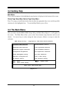
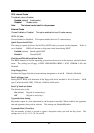
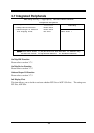
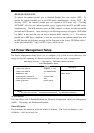
3-6-2 AGP Timing Settings
CMOS Setup Utility – Copyright(C) 1984-2003 Award Software
AGP Timing Settings
Item Help
AGP Transfer Aperture Size 64M
AGP Transfer Mode 4X
AGP Driving Control Auto
* AGP Driving Value DA
AGP Fast Write Disabled
AGP Master 1 WS Write Enabled
AGP Master 1 WS Read Enabled
CPU to AGP Post Write Disabled
AGP Delay Transaction Disabled
AGP Delay Transaction Disabled
Menu Level >>
↑↓→←
Move Enter:Select +/-/PU/PD:Value F10:Save ESC:Exit F1:General Help
F5:Previous Values F6:Optimized Defaults F7:Standard Defaults
Note: Change these settings only if you are familiar with the chipset.
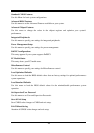
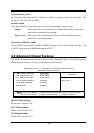
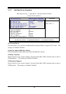
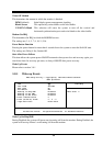
3-6-3 PCI Timing Settings
CMOS Setup Utility – Copyright(C) 1984-2003 Award Software
PCI Timing Settings
Item Help
PCI Master 1 WS Write Disabled
PCI Master 1 WS Read Disabled
CPU to AGP Post Write Enabled
PCI Delay Transaction Disabled
Menu Level >>
↑↓→←
Move Enter:Select +/-/PU/PD:Value F10:Save ESC:Exit F1:General Help
F5:Previous Values F6:Optimized Defaults F7:Standard Defaults
PCI Delay Transaction
The chipset has an embedded 32-bit posted write buffer to support delay transactions cycles.
Select Enabled to support compliance with PCI specification version 2.1. The settings are:
Enabled and Disabled.