Intel
®
Solid-State Drive 320 Series
Intel
®
Solid-State Drive 320 Series
Product Specification September 2011
14 Order Number: 325152-002US
Intel
®
Solid-State Drive 320 Series
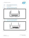
4.2 Signal Descriptions
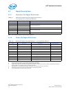
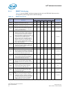
4.2.1 Connector Pin Signal Definitions
Note: Key and spacing separate signal and power segments.
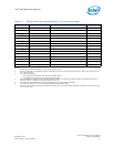
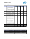
4.2.2 Power Pin Signal Definitions
Notes:
1. All mate sequences assume zero angular offset between connectors.
2. P1 and P2 are internally connected to one another within the device.
3. Ground connectors P3 and P4 may contact before the other 1st mate pins in both the power and signal connectors to
discharge ESD in a suitably configure backplane connector.
4. P5 and P6 are not connected internally to the device. The host may put 5V on these pins.
5. The host may ground P7 if it is not used for Device Activity Signal (DAS).
6. P8 and P9 should not be connected by the host.
Table 9. Serial ATA Connector Pin Signal Definitions —
1.8-inch and 2.5-inch Form Factors
Pin Function Definition
S1 Ground 1st mate
S2 A+
Differential signal pair A
S3 A-
S4 Ground 1st mate
S5 B-
Differential signal pair B
S6 B+
S7 Ground 1st mate
Table 10. Serial ATA Power Pin Definitions — 1.8-inch Form Factor
Pin Function Definition Mating Order
1
P1
2
V
33
3.3 V Power 2nd Mate
P2
2
V
33
3.3 V Power, pre-charge 2nd Mate
P3
3
Ground 1st Mate
P4
3
Ground 1st Mate
P5
4
V
5
5 V Power. Not connected 1st Mate
P6
4
V
5
5 V Power. Not connected 2nd Mate
P7
5
DAS Device Activity Signal 2nd Mate
Key Key NC NC
P8
6
Optional Manufacturing Test Pin 2nd Mate
P9
6
Optional Manufacturing Test Pin 2nd Mate


