Intel® Solid-State Drive 530 Series (2.5-inch)
October 2013 Product Specification
Order Number: 329212-003US 15
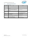
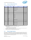
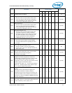
4.2.2 Power Pin Signal Definitions
Table 12: Serial ATA Power Pin Definitions
Pin
1
Name Definition Mating Order
P1
2
V
33
3.3 V Power; not used
2nd Mate
P2
2
V
33
3.3 V Power; not used
2nd Mate
P3
2
DevSleep Device Sleep Pin
1st Mate
P4
3,4
Ground
1st Mate
P5
3
Ground
1st Mate
P6
3
Ground
1st Mate
P7
3,5
V
5
5 V Power
1st Mate
P8
3,5
V
5
5 V Power
2nd Mate
P9
3,5
V
5
5 V Power
2nd Mate
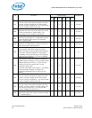
P10
3
Ground
1st Mate
P11
6
DAS Device Activity Signal
2nd Mate
P12
3, 4
Ground
1st Mate
P13
2
V
12
12 V Power; not used
1st Mate
P14
2
V
12
12 V Power; not used
2nd Mate
P15
2
V
12
12 V Power; not used
2nd Mate
Notes:
1. All pins are in a single row, with a 1.27 mm (0.050-inch) pitch.
2. Pins P1, P2 and P3 are connected together; Pins P13, P14 and P15 are connected together. Although they are not
connected internally to the device, the host may apply voltage on these pins.
3. The mating sequence is:
• Ground pins P4-P6, P10, P12 and the 5 V power pin P7.
• Signal pins and the rest of the 5 V power pins P8-P9.
4. Ground connectors P4 and P12 may contact before the other 1st mate pins in both the power and signal connectors to
discharge ESD in a suitably configured backplane connector.
5. Power pins P7, P8, and P9 are internally connected to one another within the device.
6. The host may ground P11 if it is not used for Device Activity Signal (DAS).
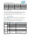
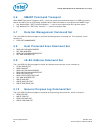
4.3 Device Sleep Feature
Device Sleep (or DevSleep/DEVSLP) is the latest feature aligned with Intel® 4th Generation Core™-
based Ultrabook™. Ultrabook™ has stringent power requirements for SSDs and as such requires an
ability to put the drive in a low power state. Although Link Power Management allows some control
over power consumption, both methods still require the SATA link to remain online. The DevSleep pin
is an enable high pin which is pulled up by the drive


