


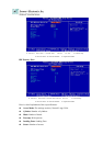

You can choice Enable, Disable and Auto.
Baud Rate The Default baud rate is 38400.
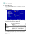
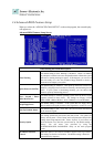
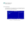
DRAM Clock This item enables you to manually set the DRAM Clock. We recommend
that you leave this item at the default value.
DRAM Timing Control Set this By SPD to enable the system to automatically set the SDRAM
timing by SPD (Serial Presence Detect). SPD is an EEPROM chip on the
DIMM module that stores information about the memory chips it contains,
including size, speed, voltage, row and column addresses, and
manufacturer.
DRAM CAS Latency (2.5) Enables you to select the CAS latency time in HCLKs of 2/2 or 3/3. The
value is set at the factory depending on the DRAM installed. Do not change
the val-ues in this field unless you change specifications of the installed
DRAM or the installed CPU. The options are "2" and "2.5" default.
Bank Interleave Enable this item to increase memory speed. When enabled, separate
memory banks are set for odd and even addresses and the next byte of
memory can be accessed while the current byte is being refreshed.
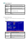
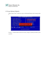
Precharge to Active
(3T/4T)
This item is used to designate the minimum Row Precharge time of the
SDRAM devices on the module.
Active to Precharge
(6T/10T)
This item specifies the number of clock cycles needed after a bank active
command before a precharge can occur.
Active to CMD (3T) This item specifies the minimum required delay between activation of
different rows.
DRAM DRAM Command
Rate (2T command)
This item enables you to specify the waiting time for the CPU to issue the
next command after issuing the command to the DDR memory. We
recommend that you leave this item at the default value.
Memory Hole At
15M-16M
You can reserve this area of system memory for ISA adapter ROM. When
this area is reserved, it cannot be cached. The user information of
peripherals that need to use this area of system memory usually discusses
their memory requirements.
System BIOS Cacheable Selecting “Enabled” allows caching of the system BIOS ROM at F0000h –
FFFFFh, resulting in better system performance. However, if any program
writes to this memory area, a system error may result. The settings are
“Enabled” and “Disabled”.
Video BIOS Cacheable Selecting Enabled allows caching of the video BIOS ROM at C0000h to
C7FFFh, resulting in better video performance. However, if any program
writes to this memory area, a system error may result.
VGA Share Memory Size Select VGA memory size