


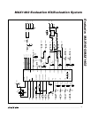
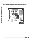
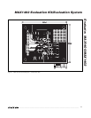
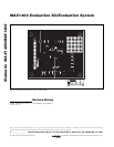

Evaluate: MAX1400/MAX1402
MAX1402 Evaluation Kit/Evaluation System
8 _______________________________________________________________________________________
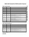
Table 4. Guide to Register Bit Functions
REGISTER BIT NAME DESCRIPTION
COMMS 0/DRDY Start bit is zero; DIN pin must be 1 when idle
RS2–RS0 Register select for subsequent operation
R/W
Selects subsequent read or write operation
RESET Causes software reset when set to 1
STDBY Activates standby power-down mode when set to 1
FSYNC Inhibits the A/D converter when set to 1
GS1 A1 Selects the active channel
A0 Selects the active channel
MF1 Selects the data output rate
MF0 Selects the data output rate
CLK Selects the CLKIN frequency
FS1 Select the data output rate
FS0 Select the data output rate
FAST Selects SINC
1
filter instead of SINC
3
GS2 SCAN Enables the scanning sequences
M1 Enables the CalGain channel
M0 Enables the CalOff channel
BUFF Enables the input buffers
DIFF Selects differential input pairs
BOUT Enables the transducer burn-out test currents
IOUT Enables the OUT1 and OUT2 current sources (MAX1402 only)
X2CLK Selects the CLKIN frequency
SFR MDOUT
Changes the DOUT and INT pins to provide raw modulator output
FULLPD Activates full power-down mode. Use hardware reset to restore normal operation.
All other bits in SFR must be zero
TF1, 2, 3 G2–G0 Select the PGA Gain
U/B
Selects unipolar or bipolar coding
D3–D0 Select the offset correction DAC code; D3 = sign, D2–D0 = magnitude
DATA D17–D0 Raw code value
DS1 Value of the DS1 input pin (MAX1402 only)
DS0 Value of the DS0 input pin (MAX1402 only)
CID2–CID0 Channel identification tag