


3-20
MS-7563 Mainboard
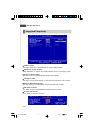
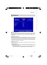
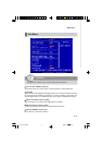
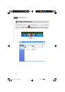
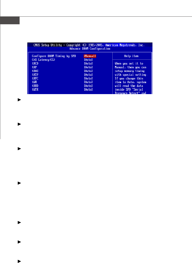
Configure DRAM Timing by SPD
Setting to [Enabled] enables DRAM CAS# Latency automatically to be determined
by BIOS based on the configurations on the SPD (Serial Presence Detect) EEPROM
on the DRAM module.
CAS Latency(CL)
When the Configure DRAM Timing by SPD sets to [Manual], the field is
adjustable.This controls the CAS latency, which determines the timing delay (in
clock cycles) before SDRAM starts a read command after receiving it.
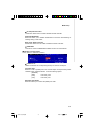
tRCD
When the Configure DRAM Timing by SPD sets to [Manual], the field is
adjustable. When DRAM is refreshed, both rows and columns are addressed
separately. This setup item allows you to determine the timing of the transition
from RAS (row address strobe) to CAS (column address strobe). The less the
clock cycles, the faster the DRAM performance.
tRP
When the Configure DRAM Timing by SPD sets to [Manual], this field is
adjustable. This setting controls the number of cycles for Row Address Strobe
(RAS) to be allowed to precharge. If insufficient time is allowed for the RAS to
accumulate its charge before DRAM refresh, refresh may be incomplete and
DRAM may fail to retain data. This item applies only when synchronous DRAM is
installed in the system.
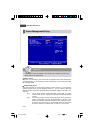
tRAS
When the Configure DRAM Timing by SPD sets to [Manual], this setting
determines the time RAS takes to read from and write to a memory cell.
tRTP
When the Configure DRAM Timing by SPD sets to [Manual], this setting
controls the time interval between a read and a precharge command.
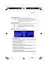
tRFC
When the Configure DRAM Timing by SPD sets to [Manual], the field is
adjustable. The row cycle time determines the minimum number of clock cycles
a memory row takes to complete a full cycle, from row activation up to the
precharging of the active row.
7563v1.0-3_BIOS.p65 2008/11/11, 下午 05:3620