


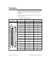
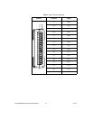
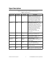
© National Instruments Corporation 17 NI USB-6008/6009 User Guide and Specifications
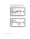
Minimizing Glitches on the Output Signal
When you use a DAC to generate a waveform, you may observe glitches in
the output signal. These glitches are normal; when a DAQ switches from
one voltage to another, it produces glitches due to released charges. The
largest glitches occur when the most significant bit of the DAC code
changes. You can build a lowpass deglitching filter to remove some of
these glitches, depending on the frequency and nature of the output signal.
Refer to
ni.com/support for more information about minimizing
glitches.
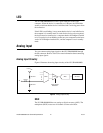
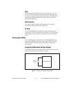
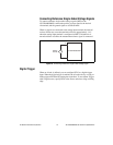
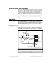
Digital I/O
The NI USB-6008/6009 has 12 digital lines, P0.<0..7> and P1.<0..3>,
which comprise the DIO port. GND is the ground-reference signal for the
DIO port. You can individually program all lines as inputs or outputs.
Digital I/O Circuitry
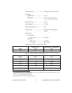
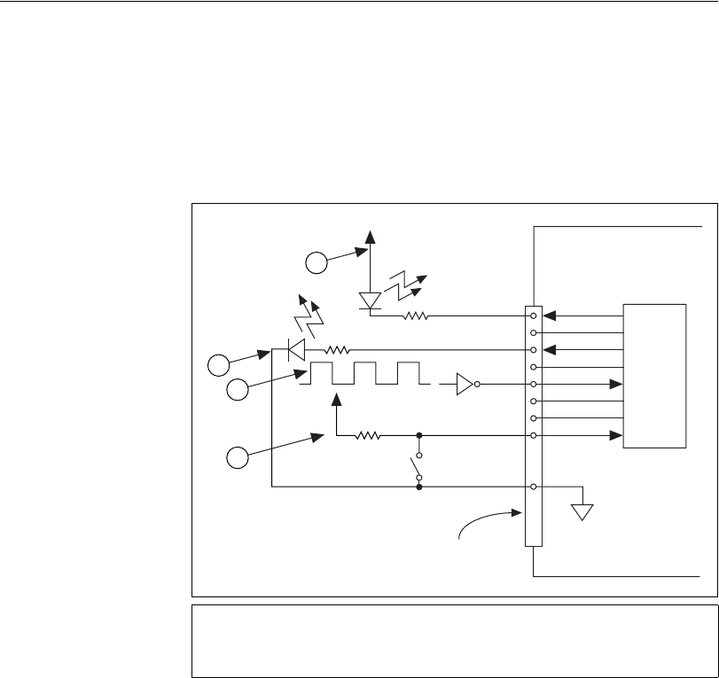
Figure 13 shows P0.<0..7> connected to example signals configured as
digital inputs and digital outputs. You can configure P1.<0..3> similarly.
Figure 13. Example of Connecting a Load
1 P0.0 configured as an open collector digital output driving a LED
2 P0.2 configured as a active drive digital output driving a LED
3 P0.4 configured as a digital input receiving a TTL signal from a gated invertor
4 P0.7 configured as a digital input receiving a 0 V or 5 V signal from a switch
+5 V
LED
Switch
I/O Connector
GND
P0.0
P0.1
P0.2
P0.3
P0.4
P0.5
P0.6
P0.7
+5 V
LED
1
2
3
4
TTL Signal