


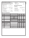


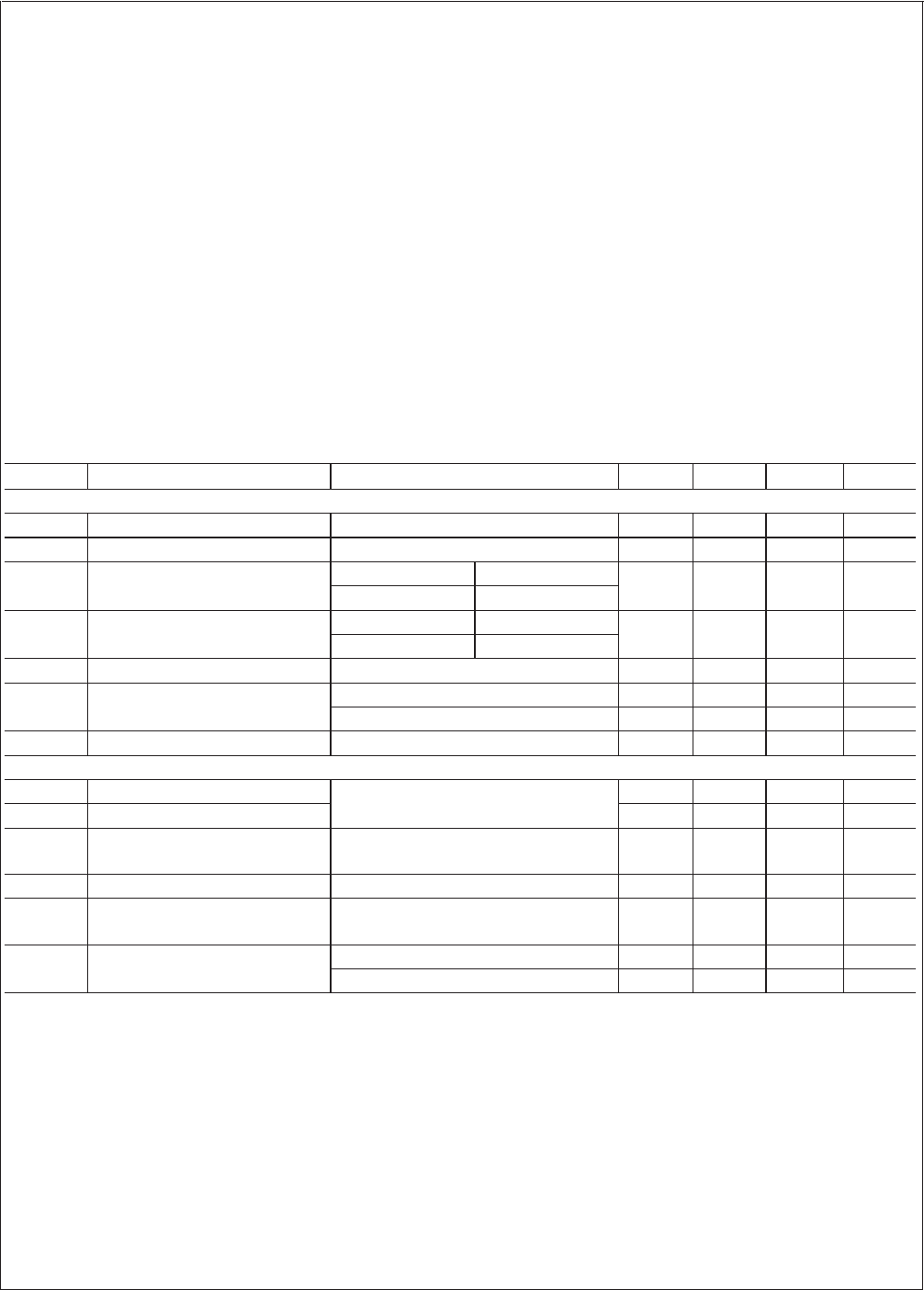
Absolute Maximum Ratings (Note 1)
If Military/Aerospace specified devices are required,
please contact the National Semiconductor Sales Office/
Distributors for availability and specifications.
Supply Voltage (V
DD
) −0.3V to +4V
LVCMOS/LVTTL Input
Voltage −0.3V to (V
DD
+ 0.3V)
LVCMOS/LVTTL Output
Voltage −0.3V to (V
DD
+ 0.3V)
LVDS Receiver Input Voltage −0.3V to (V
DD
+ 0.3V)
Junction Temperature +150˚C
Storage Temperature −65˚C to +150˚C
Lead Temperature
(Soldering, 10 sec.) +260˚C
Maximum Package Power Dissipation Capacity
@
25˚C
128 TQFP Package: 1.4W
Package Derating: 25.6mW/˚C above +25˚C
ESD Rating:
(HBM, 1.5kΩ, 100pF)
>
2kV
(EIAJ, 0Ω, 200pF)
>
200 V
Recommended Operating
Conditions
Min Nom Max Units
Supply Voltage (V
DD
) 3.15 3.3 3.6 V
Operating Free Air
Temperature (T
A
) 0 +25 +70 ˚C
Supply Noise Voltage (V
P-P
)
±
100 mV
p-p
Receiver Input Range 0 V
DD
V
Input Clock Frequency (f) 8 135 MHz
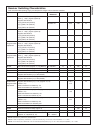
Electrical Characteristics
Over recommended operating supply and temperature ranges unless otherwise specified.
Symbol Parameter Conditions Min Typ Max Units
CMOS/TTL DC SPECIFICATIONS (Rx outputs, control inputs and outputs)
V
IH
High Level Input Voltage 2.0 V
DD
V
V
IL
Low Level Input Voltage 0 0.8 V
V
OH
High Level Output Voltage Rx clock out I
OH
=−4mA 2.4 V
Rx data out I
OH
=−2mA
V
OL
Low Level Output Voltage Rx clock out I
OL
=+4mA 0.4 V
Rx data out I
OL
=+2mA
V
CL
Input Clamp Voltage I
CL
= −18 mA −0.8 −1.5 V
I
IN
Input Current V
IN
=V
DD
+10 µA
V
IN
= 0V −10 µA
I
OS
Output Short Circuit Current V
OUT
= 0V −120 mA
LVDS RECEIVER DC SPECIFICATIONS
V
TH
Differential Input High Threshold V
CM
= +1.2V +100 mV
V
TL
Differential Input Low Threshold −100 mV
V
IN
Input Voltage Range
(Single-ended)
0V
DD
V
|V
ID
| Differential Input Voltage 0.200 0.600 V
V
CM
Differential Common Mode
Voltage
0.2 1.2 V
DD
−0.1 V
I
IN
Input Current V
IN
= +2.4V, V
DD
= 3.6V
±
10 µA
V
IN
= 0V, V
DD
= 3.6V
±
10 µA
DS90C3202
www.national.com3