


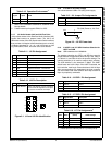

www.national.com 8 (Confidential) Revision 0.2
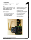
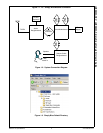
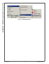
LMX9820ADEV: LMX9820A Simply Blue Module Kit User’s Guide
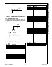
2.1.1 Schmitt Trigger for POR (Power On Reset)
A Schmitt Trigger for POR has been added to the Texas
Motherboard to allow control of delay between VCC/IOVCC
and RESET#. A minimum of 2 ms is required between
VCC/IOVCC at rail and RESET# transition from low to high
to have proper startup of the module.
2.1.2 P3 DP9 Serial Connector
P3 is a DP9 serial port connector that interfaces to the
LMX9820A’s full duplex UART. It supports up to 921.6 kbps
transfer rates. Refer to Table 2-4 for selecting and setting
the UART and transfer rate.
2.1.3 JP1 JTAG Connector
JP1 is a JTAG based serial on-chip debug interface. The
JTAG interface allows the user fast program code download
into the on-chip Flash program memory (e.g., firmware
updates could be done via this interface).
2.1.4 J4 Test Points and General Purpose Output
J4 is a test point header and general purpose output con-
nector. Test points are for internal use only and general
purpose outputs are not currently utilized, not configured in
firmware.
2.1.5 J5 USB Connector
Note: Not used for LMX9820A.
J5 is a USB (female), PCB mounting, 90° angled connector
that interfaces with the USB transport layer in baseband.
The on-chip USB module is compatible with USB specifica-
tions v1.0 and 1.1.
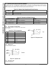
2.1.6 Mode Selection/ISP (In-System Programming)
Configuration Header
Programming of the internal Flash can either be done over
the JTAG interface or by starting a special ISP code,
located in the boot area of the Flash. For normal Bluetooth
operation, no jumpers are required on J6 or J7.
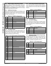
Table 2-4. P1 DP9 Pin Assignments
Pin # Signal Name Description
1 NC No Connect
2
RDX UART Receive Data input
3
TDX UART Transmit Data output
4
NC No Connect
5
GND Ground
6
NC No Connect
7
RTS# UART Ready-To-Send output
8
CTS# UART Clear-To-Send input
9
NC No Connect
Table 2-5. JP1 JTAG Connector Pin Assignments
Pin # Signal Name Description
1 RESET# Reset - active low
2
IOVCC IOVCC
3 NC No Connect
4
GND Ground
5
NC No Connect
6
GND Ground
7
TMS JTAG Test Mode Select
8
GND Ground
9
TDI JTAG Test Data input
10
GND Ground
11
TCK JTAG Test Clock input
12
GND Ground
13
TDO JTAG Test Data output
14
GND Ground
15
NC No Connect
16
GND Ground
17
NC No Connect
18
GND Ground
19
RDY# JTAG Test Ready output - active low
20
NC No Connect
Table 2-6. J4 Pin Assignment
Pin # Signal Name Description
1 TIO4_BB Test Point - internal use only
2
TIO3_BB Test Point - internal use only
3
GPO2 General Purpose Output - not currently
utilized
4
GPO1 General Purpose Output - not currently
utilized
Table 2-7. J5 Pin Assignment
Pin # Signal Name Description
1
UVCC_5V VCC USB
2
D- USB D- upstream port
3
D+ USB D+ upstream port
4
GND Ground USB
Table 2-8. J6 Pin Assignments
Pin # Signal Name Description
1
GND Ground
2
ENV0 Refer to Table 2-10 for logic matrix
3
IOVCC VCC
Table 2-9. J7 Pin Assignments
Pin # Signal Name Description
1 GND Ground
2
ENV1 Refer to Table 2-10 for logic matrix
3
IOVCC VCC