


Revision 0.2 (Confidential) 9 www.national.com
LMX9820ADEV: LMX9820A Simply Blue Module Kit User’s Guide
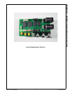
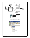
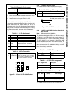
2.1.7 J12 Audio Header (4x2) and J23 Test Point
J12 provides access to the Advanced Audio Interface (AAI)
signals that connect an external codec. The AAI is an
advanced version of the SSI (Synchronous Serial Interface)
that provides a full-duplex communications port to a variety
of industry-standard 13-, 14-, 15-, and 16-bit linear or 8-bit
log PCM codecs, DSPs, and other serial audio devices.
Figure 2-1. J12 and J23 Pin Identification
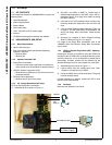
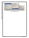
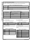
2.1.8 J14 USB or DC Power Supply
J14 selects between USB or DC (wall) power supply.
Figure 2-2. J15 DC Power Jack
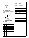
2.1.9 J16 ISEL1 and J17 ISEL2 Interface Selection for
UART and USB
Note: USB is not used for LMX9820A.
The interface selection pins ISEL1 and ISEL2 are used to
provide different configurations after boot-up. See Table 2-
14, Table 2-15, and Table 2-16 for the specific settings. The
interface selection pin is used for transport layer selection.
The USB interface is the standard 12 Mbps. The UART
default baud rate is 921.6 kbps. If the UART is selected, the
host controller must begin communications at 921.6 kbps.
After communications are established, the host controller
can then select baud rates between 38.4 kbps and 921.6
kbps via proprietary commands.
Table 2-10. Operation Environment
1
1. Refer to the LMX9820A datasheet for additional mode
boot-up details.
ENV0
Input
ENV1
Input Mode
0 1 ISP Firmware Upgrade
11
Normal Operation
2
2. A weak internal pull-up pulls ENV0/1 to VCC.
Table 2-11. J12 Pin Assignment
Pin # Signal Name Description
1 GND Ground
2
SCK AAI Clock
3
VCC
VCC
4
SFS AAI Frame Synchronization
5
J23 Optional Test Point - user defined
6
STD AAI Transmit Data output
7
GND Ground
8
SRD AAI Receive Data input
Table 2-12. J23 Pin Description
Pin # Signal Name Description
1 User Defined J23 is user defined. Can be connected
to one of the AAI signals for a test point
or used for an external clock input.
2
4
6
8
1
3
5
7
J23
J12
Table 2-13. J14 Jumper Pin Assignments
Pin # Description
1-2 USB Power
2-3
DC (wall) Power Supply
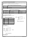
Table 2-14. J16 ISEL1 Pin Assignment
Pin # Signal Name Description
1 IOVCC IOVCC
2
ISEL1 ISEL1
3
GND Ground
Table 2-15. J17 ISEL2 Pin Assignment
Pin # Signal Name Description
1 IOVCC IOVCC
2
ISEL2 ISEL2
3
GND Ground
Table 2-16. J17 Pin Assignments
1
1. Default pins are internally set to 1 by weak pull-up.
ISEL1 ISEL2
Interface Speed
(baud) UART Settings
1 1 921.6 Check NVS
0 1 115.2 Check NVS
1 0 9.6 k No parity, one stop bit
0 0 Check NVS Check NVS
J15
1
2
DC (Wall) Power to J14, Pin 3