266
¡ SemiconductorMSM80C154S/83C154S
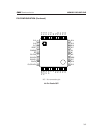
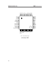
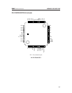
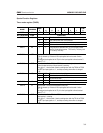
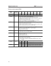
P0.0 to P0.7
P1.0 to P1.7
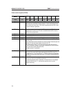
P2.0 to P2.7
P3.0 to P3.7
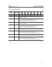
ALE
PSEN
EA
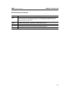
Symbol Descriptipn
Bidirectional I/O ports. They are also the data/address bus (input/output of data and output of
lower 8-bit address when external memory is accessed).
They are open-drain outputs when used as I/O ports, but 3-state outputs when used as data/address
bus.
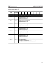
P1.0 to P1.7 are quasi-bidirectional I/O ports. They are pulled up internally when used as input
ports. Two of them have the following secondary functions:
•P1.0 (T2)
•P1.1 (T2EX)
: used as external clock input pins for the timer/counter 2.
: used as trigger input for the timer/counter 2 to be reloaded or captured;
causing the timer/counter 2 interrupt.
P2.0 to P2.7 are quasi-bidirectional I/O ports. They also output the higher 8-bit address when
an external memory is accessed. They are pulled up internally when used as input ports.
P3.0 to P3.7 are quasi-bidirectional I/O ports. They are pulled up internally when used as input
ports. They also have the following secondary functions:
•P3.0 (RXD)
Serial data input/output in the I/O expansion mode and serial data input in the UART mode when
the serial port is used.
•3.1 (TXD)
Synchronous clock output in the I/O expansion mode and serial data output in the UART mode
when the serial port is used.
•3.2 (INT0)
Used as input pin for the external interrupt 0, and as count-up control pin for the timer/counter 0.
•3.3 (INT1)
Used as input pin for the external interrupt 1, and as count-up control pin for the timer/counter 1.
•3.4 (T0)
Used as external clock input pin for the timer/counter 0.
•3.5 (T1)
Used as external clock input pin for the timer/counter 1 and power-down-mode control input pin.
•3.6 (WR)
Output of the write-strobe signal when data is written into external data memory.
•3.7 (RD)
Output of the read-strobe signal when data is read from external data memory.
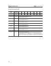
Address latch enable output for latching the lower 8-bit address during external memory access.
Two ALE pulses are activated per machine cycle except during external data memory access at
which time one ALE pulse is skipped.
Program store enable output which enables the external memory output to the bus during external
program memory access. Two PSEN pulses are activated per machine cycle except during
external data memory access at which two PSEN pulses are skipped.
When EA is held at "H" level, the MSM 83C154S executes instructions from internal program
memory at address 0000H to 3FFFH, and executes instructions from external program memory
above address 3FFFH.
When EA is held at "L" level, the MSM80C154S/MSM83C154S executes instructions from external
program memory for all addresses.
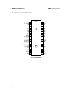
PIN DESCRIPTIONS


