


Chip RC Networks
Design and specifi cations are each subject to change without notice. Ask factory for the current technical specifi cations before purchase and/or use.
Should a safety concern arise regarding this product, please be sure to contact us immediately.
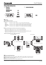
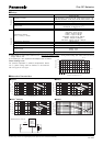
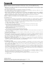
GND
Electrode
(Outer)
Marking
Protective coating
Alumina substrate
Electrode
(Outer)
GND
Electrode
(Outer)
33
GND
Electrode
(Outer)
Marking
Protective coating
Alumina substrate
Electrode
(Outer)
GND
Electrode
(Outer)
GND
Electrode
(Outer)
Marking
Protective coating
Alumina substrate
Electrode
(Outer)
GND
Electrode
(Outer)
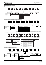
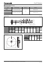
R1
C1
R2
C2
R3 R4
C3 C4
10 9 8 7
2345
61
R1=R2=R3=R4
C1=C2=C3=C4
GND GND
R1
C1
R2
C2
R3 R4
C3
C4
10 9 8 7
234561
GNDGND R1=R2=R3=R4
C1=C2=C3=C4
1112
GND
Electrode
(Outer)
Marking
Protective coating
Alumina substrate
Electrode
(Outer)
GND
Electrode
(Outer)
33
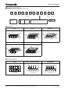
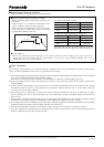
E
1
Z
2
A
3
S
4
S
5
B
6
7
7
0
8
1
9
A
10
J
11 12
SSB
J ±5%
4.0 mm
҂2.1 mm
Thick Film Noise
Suppression and
Filtering
Components
Suffix for Special
Requirement
Dimension and
Circuit Configuration
Resistance
Tolerance
Design Number
Common Code
Convex
terminal type
Chip RC
Networks
Resistance Value : 10 ȑ to 100 kȑ
Capacitance Value : 10 pF to 180 pF
In above-mentioned range, it is possible to
choose optional R/C.
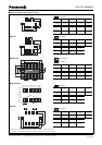
GND
Electrode
(Outer)
Marking
Protective coating
Alumina substrate
Electrode
(Outer)
R1 R2 R3 R4
C1 C2 C3 C4
10 9 8 7
GND GND
2345
61
R1=R2=R3=R4
C1=C2=C3=C4
■ Explanation of Part Numbers
● EZASSB (R/C Except the standard Com bi na tion)
■ Construction
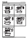
■ Circuit Confi guration
EZACT EZADT EZAST/SS
EZANT EZASTB/SSB
EZACT EZADT
•
EZAST/SS
•
EZANT EZASTB/SSB
Feb. 2006