


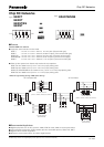

Chip RC Networks
Design and specifi cations are each subject to change without notice. Ask factory for the current technical specifi cations before purchase and/or use.
Should a safety concern arise regarding this product, please be sure to contact us immediately.
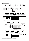
GND
c
f2
f1
a
e
d
b P
Land pattern
Solder resistant
GND
f2
f1
a
Pc db
Land pattern
Land pattern
Pb
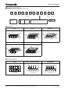
f
a
g
c
d
f
a
g
c
d
P
b
Land pattern
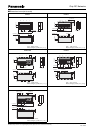
e
a
h
g
c
Pb
d
Land pattern
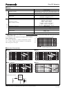
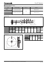
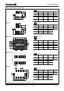
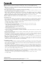
■ Recommended Land Pattern Design
●
EZAST/SS
●
EZACT
●
EZASTB/SSB
●
EZANT
• Design to make GND pattern as large as possible, because high
frequency noise is removed from GND terminals of chip RC network.
abcd
Dimensions
(mm)
1.2 to 1.4 0.4 3.1 to 3.3 0.4 to 0.5
ef1f2P
Dimensions
(mm)
0.8 2.9 to 3.3 4.8 to 5.2 0.8
abcd
Dimensions
(mm)
0.75 0.25 1.70 0.35
ehgP
Dimensions
(mm)
1.85 2.60 0.25 0.60
abcd
Dimensions
(mm)
1.4 to 1.6 0.35 0.45 0.3
f1 f2 P
Dimensions
(mm)
2.7 to 3.5 3.8 0.65
abcd
Dimensions
(mm)
2.3 to 2.5 0.4 to 0.6 5.6 to 5.8 0.4 to 0.8
fgP
Dimensions
(mm)
4.3 to 4.7 7.6 to 8.0 1.27
●
EZADT
abcd
Dimensions
(mm)
0.9 to 1.1 0.2 to 0.3 2.6 to 2.8 0.3 to 0.4
fgP
Dimensions
(mm)
2.0 to 2.6 3.6 to 4.2 0.635
Feb. 2006