


Philips Semiconductors Product data
CBT338410-bit bus switch with 5-bit output enables
2001 Dec 20
3
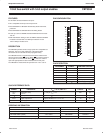
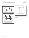
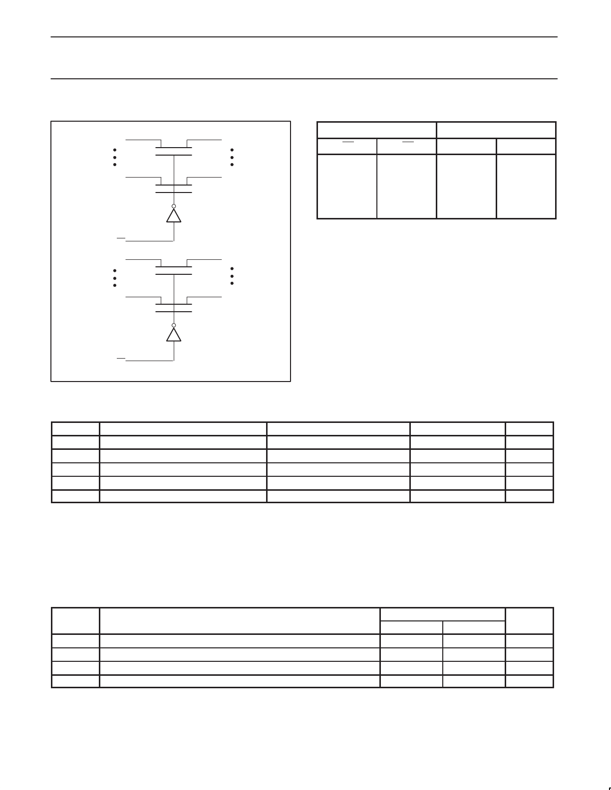
LOGIC SYMBOL
1A1
1A5
2A1
2A5
1B1
1B5
2B1
2B5
3
11
2
10
14
22
15
23
SA00555
13
1
2OE
1OE
FUNCTION TABLE
INPUTS OUTPUTS
1OE 2OE 1A, 1B 2A, 2B
L L 1A = 1B 2A= 2B
L H 1A = 1B Z
H L Z 2A = 2B
H H Z Z
H = High voltage level
L = Low voltage level
Z = High impedance “off” state
ABSOLUTE MAXIMUM RATINGS
1,
2
SYMBOL
PARAMETER CONDITIONS RATING UNIT
V
CC
DC supply voltage –0.5 to +7.0 V
I
IK
DC input diode current –50 mA
V
I
DC input voltage
3
–1.2 to +7.0 V
I
SW
DC output diode current V
O
< 0 ±128 mA
T
stg
Storage temperature range –65 to +150 °C
NOTES:
1. Stresses beyond those listed may cause permanent damage to the device. These are stress ratings only and functional operation of the
device at these or any other conditions beyond those indicated under “recommended operating conditions” is not implied. Exposure to
absolute-maximum-rated conditions for extended periods may affect device reliability.
2. The performance capability of a high-performance integrated circuit in conjunction with its thermal environment can create junction
temperatures which are detrimental to reliability. The maximum junction temperature of this integrated circuit should not exceed 150 °C.
3. The input and output voltage ratings may be exceeded if the input and output current ratings are observed.
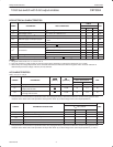
RECOMMENDED OPERATING CONDITIONS
SYMBOL
PARAMETER
LIMITS
UNIT
SYMBOL
PARAMETER
Min Max
UNIT
V
CC
DC supply voltage 4.5 5.5 V
V
IH
High-level input voltage 2.0 — V
V
IL
Low-level Input voltage — 0.8 V
T
amb
Operating free-air temperature range –40 +85 °C