


Philips Semiconductors Product data
CBT6800
10-bit bus switch with precharged outputs
for live insertion
2003 Sep 12
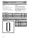
4
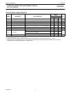
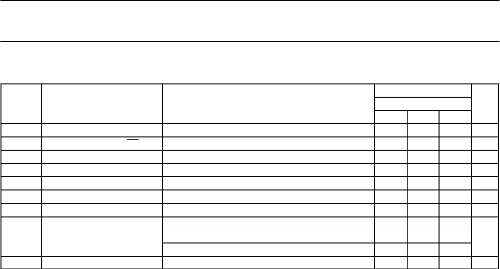
DC ELECTRICAL CHARACTERISTICS
LIMITS
SYMBOL PARAMETER TEST CONDITIONS
T
amb
= -40 to +85 °C
UNIT
Min Typ
1
Max
V
IK
Input clamp voltage V
CC
= 4.5 V; I
I
= -18 mA — — -1.2 V
I
I
Input leakage current - OE V
CC
= 5.5 V; V
I
= GND or 5.5 V — — ±5 µA
I
O
Output bias current V
CC
= 4.5 V; BiasV = 2.4 V; V
O
= 0 0.25 — — mA
I
CC
Quiescent supply current V
CC
= 5.5 V; I
O
= 0, V
I
= V
CC
or GND — — 50 µA
∆I
CC
Control pins
2
V
CC
= 5.5 V, one input at 3.4 V, other inputs at V
CC
or GND — — 2.5 mA
C
I
Control pins V
I
= 3 V or 0 — 3.5 — pF
C
O(OFF)
Off-state capacitance - I/O pins V
O
= 3 V or 0; switch off — 8.2 — pF
V
CC
= 4.5 V; V
I
= 0 V; I
I
= 64 mA — 5 7
r
on
3
On-resistance
V
CC
= 4.5 V; V
I
= 0 V; I
I
= 30 mA — 5 7
Ω
on
V
CC
= 4.5 V; V
I
= 2.4 V; I
I
= 15 mA — 10 15
VP Pass gate voltage V
IN
= V
CC
= 5.0 V, I
OUT
= -100 µA 3.4 3.6 3.9 V
NOTES:
1. All typical values are at V
CC
= 5 V, T
amb
= 25 °C
2. This is the increase in supply current for each input that is at the specified TTL voltage level rather than V
CC
or GND
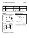
3. Measured by the voltage drop between the A and the B terminals at the indicated current through the switch. On-state resistance is
determined by the lowest voltage of the two (A or B) terminals.