


Philips Semiconductors Product data
CBT6800
10-bit bus switch with precharged outputs
for live insertion
2003 Sep 12
5
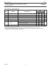
AC CHARACTERISTICS
GND = 0 V; C
L
= 50 pF; t
r
= t
f
≤ 2.5 ns
LIMITS
SYMBOL PARAMETER
FROM TO
V
CC
= +5.0 V ±0.5 V
UNIT
(INPUT) (OUTPUT)
Min Max
t
pd
Propagation delay
1
A or B B or A — .25 ns
t
PZH
T
PZL
BIASV = GND
BIASV = 3 V
ON A or B
2.4
3.0
7.7
8.3
ns
t
PHZ
T
PLZ
BIASV = GND
BIASV = 3 V
ON A or B
1.0
3.1
5.3
7.8
ns
NOTE:
1. This parameter is warranted but not production tested. The propagation delay is based on the RC time constant of the typical on-state
resistance of the switch and a load capacitance of 50 pF, when driven by an ideal voltage source (zero output impedance).
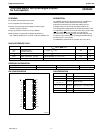
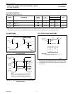
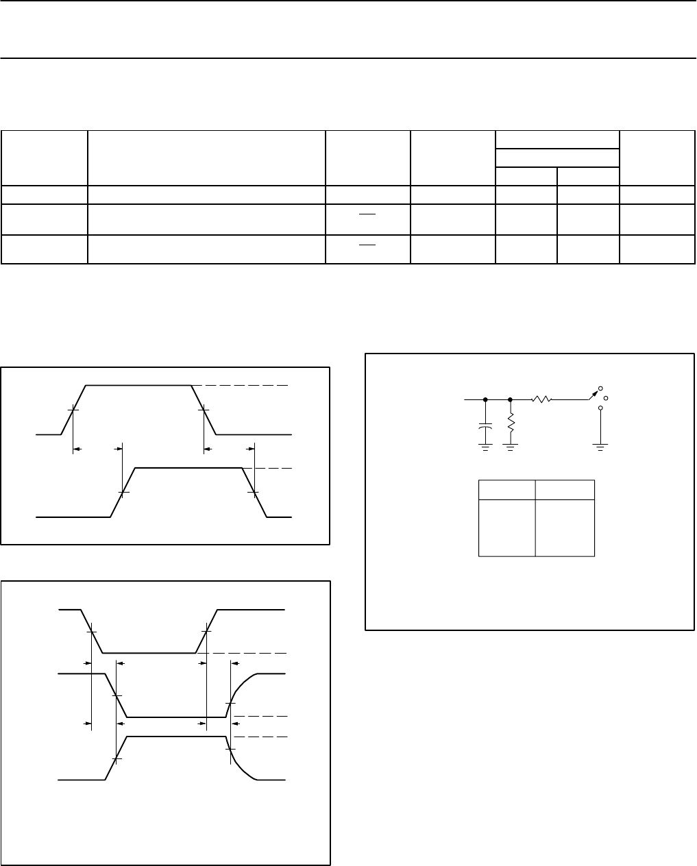
AC WAVEFORMS
V
M
= 1.5 V, V
IN
= GND to 3.0 V
INPUT
1.5V
OUTPUT
t
PLH
t
PHL
SA00028
1.5V
1.5V 1.5V
3 V
0 V
V
OH
V
OL
Waveform 1. Waveforms Showing the Input (An) to Output (Yn)
Propagation Delays
Output Control
(Low-level
enabling
1.5 V
t
PZH
t
PHZ
V
OH
V
OL
t
PZL
t
PLZ
3.5V
0V
V
OL
+ 0.3V
V
OH
- 0.3V
SA00029
1.5 V
1.5 V 1.5 V
0V
3V
Output
Waveform 1
S1 at 7 V
(see Note)
Note:
Waveform 1 is for an output with internal conditions such that
the output is low except when disabled by the output control.
Waveform 2 is for an output with internal conditions such that
the output is high except when disabled by the output control.
Output
Waveform 2
S1 at Open
(see Note)
Waveform 2. Waveforms Showing the 3-State Output Enable
and Disable Times
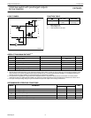
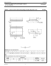
TEST CIRCUIT AND WAVEFORMS
C
L
= 50 pF
500 Ω
Load Circuit
DEFINITIONS
C
L
= Load capacitance includes jig and probe capacitance;
see AC CHARACTERISTICS for value.
TEST S1
t
pd
open
t
PLZ
/t
PZL
7 V
t
PHZ
/t
PZH
open
SA00012
500 Ω
From Output
Under Test
S1
7 V
Open
GND
NOTES:
1. All input pulses are supplied by generators having the following
characteristics: PRR ≤ 10 MHz, Z
O
= 50 Ω, t
r
≤ 2.5 ns, t
f
≤ 2.5 ns.
2. The outputs are measured one at a time with one transition per
measurement.