


Philips Semiconductors Product specification
TOPFET dual high side switch PIP3207-DC
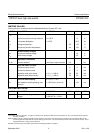
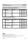
THERMAL CHARACTERISTIC
SYMBOL PARAMETER CONDITIONS MIN. TYP. MAX. UNIT
Thermal resistance
1
R
th j-mb
Junction to mounting base per channel - 2.4 3 K/W
both channels - 1.2 1.5 K/W
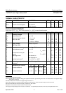
STATIC CHARACTERISTICS
Limits are at -40˚C ≤ T
mb
≤ 150˚C and typicals at T
mb
= 25 ˚C unless otherwise stated
SYMBOL PARAMETER CONDITIONS MIN. TYP. MAX. UNIT
Clamping voltages
V
BG
Battery to ground I
G
= 1 mA 45 55 65 V
V
BL
Battery to load per channel I
L
= I
G
= 1 mA 50 55 65 V
V
GL
Ground to load
2
I
L
= 10 mA 18 23 28 V
I
L
= 10 A; t
p
= 300 µs202530V
Supply voltage battery to ground
V
BG
Operating range
3
- 5.5 - 35 V
Currents 9 V ≤ V
BG
≤ 35 V
I
B
Total quiescent current
4
V
LG
= 0 V - - 20 µA
T
mb
= 25˚C - 0.1 1 µA
I
L
Off-state load current per V
BL
= V
BG
--10µA
channel T
mb
= 25˚C - 0.1 1 µA
I
G
Operating current one channel on - 1.8 3 mA
both channels on - 3.6 6 mA
I
L
Nominal load current
5
V
BL
= 0.5 V; T
mb
= 85˚C 8 - - A
R
G
Effective internal ground I
G
= -200 mA; t
p
= 300 µs 40 75 100 Ω
resistance
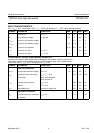
6
Resistances per channel V
BG
I
L
t
p
7
T
j
R
ON
On-state resistance 9 to 35 V 10 A 300 µs 25˚C - 30 40 mΩ
150˚C - 60 80 mΩ
R
ON
On-state resistance 5.5 V 5 A 300 µs 25˚C - 50 60 mΩ
150˚C - 100 120 mΩ
1 Of the output Power MOS transistors.
2 For a high side switch, the load pin voltage goes negative with respect to ground during the turn-off of an inductive load. This negative voltage
is clamped by the device.
3 On-state resistance is increased if the supply voltage is less than 7 V.
4 This is the continuous current drawn from the battery when both inputs are low and includes leakage currents to the loads.
5 Per channel but with both channels conducting. Defined as in ISO 10483-1.
6 Equivalent of the parallel connected resistors for both channels.
7 The supply and input voltage for the R
ON
tests are continuous. The specified pulse duration t
p
refers only to the applied load current.
September 2001 3 Rev 1.100