


512 Kbit / 1 Mbit 3.0 Volt-only, Serial Flash Memory
With 25 MHz SPI Bus Interface
PMC
FEATURES
Single Power Supply Operation
- Low voltage range: 2.7 V - 3.6 V
• Memory Organization
- Pm25LV512: 64K x 8 (512 Kbit)
- Pm25LV010: 128K x 8 (1 Mbit)
Cost Effective Sector/Block Architecture
- Uniform 4 Kbyte sectors
- Uniform 32 Kbyte blocks (8 sectors per block)
- Two blocks with 32 Kbytes each (512 Kbit)
- Four blocks with 32 Kbytes each (1 Mbit)
- 128 pages per block
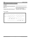
Serial Peripheral Interface (SPI) Compatible
- Supports SPI Modes 0 (0,0) and 3 (1,1)
High Performance Read
- 25 MHz clock rate (maximum)
Page Mode for Program Operations
- 256 bytes per page
Block Write Protection
- The Block Protect (BP1, BP0) bits allow part or entire
of the memory to be configured as read-only.
Hardware Data Protection
- Write Protect (WP#) pin will inhibit write operations
to the status register
• Page Program (up to 256 Bytes)
- Typical 2 ms per page program time
• Sector, Block and Chip Erase
- Typical 40 ms sector/block/chip erase time
Single Cycle Reprogramming for Status Register
- Build-in erase before programming
High Product Endurance
- Guarantee 100,000 program/erase cycles per single
sector (preliminary)
- Minimum 20 years data retention
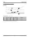
Industrial Standard Pin-out and Package
- 8-pin JEDEC SOIC
- 8-contact WSON
- Optional lead-free (Pb-free) packages
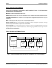
GENERAL DESCRIPTION
The Pm25LV512/010 are 512 Kbit/1 Mbits 3.0 Volt-only serial Flash memories. These devices are designed to use
a single low voltage, range from 2.7 Volt to 3.6 Volt, power supply to perform read, erase and program operations.
The devices can be programmed in standard EPROM programmers as well.
The device is optimized for use in many commercial applications where low-power and low-voltage operation are
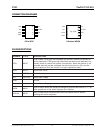
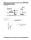
essential. The Pm25LV512/010 is enabled through the Chip Enable pin (CE#) and accessed via a 3-wire interface
consisting of Serial Data Input (Sl), Serial Data Output (SO), and Serial Clock (SCK). All write cycles are com-
pletely self-timed.
Block Write protection for top 1/4, top 1/2 or the entire memory array (1M) or entire memory array (512K) is enabled
by programming the status register. Separate write enable and write disable instructions are provided for additional
data protection. Hardware data protection is provided via the WP pin to protect against inadvertent write attempts
to the status register. The HOLD pin may be used to suspend any serial communication without resetting the serial
sequence.
Programmable Microelectronics Corp.
1
Issue Date: February, 2004, Rev: 1.4
Pm25LV512 / Pm25LV010
The Pm25LV512/010 are manufactured on PMC’s advanced nonvolatile CMOS technology, P-FLASH™. The de-
vices are offered in 8-pin JEDEC SOIC and 8-contact WSON packages with operation frequency up to 25 MHz.