10
Programmable Microelectronics Corp. Issue Date: February, 2004, Rev: 1.4
PMC Pm25LV512/010
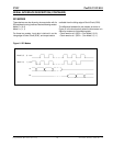
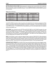
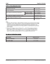
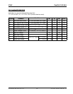
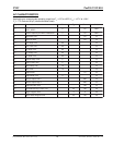
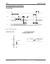
READ: Reading the Pm25LV512/010 via the SO (Serial Output) pin requires the following sequence. After the CE#
line is pulled low to select a device, the READ instruction is transmitted via the Sl line followed by the byte address
to be read (Refer to Table 7). Upon completion, any data on the Sl line will be ignored. The data (D7-D0) at
the specified address is then shifted out onto the SO line. If only one byte is to be read, the CE# line should be
driven high after the data comes out. The READ instruction can be continued since the byte address is automati-
cally incremented and data will continue to be shifted out. For the Pm25LV512/010, when the highest address is
reached, the address counter will roll over to the lowest address allowing the entire memory to be read in one
continuous READ instruction.
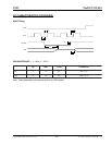
FAST_READ: The device is first selected by driving CE# low. The FAST READ instruction is followed by a 3-byte
address (A23-A0) and a dummy byte, each bit being latched-in during the rising edge of SCK (Serial Clock). Then
the memory contents, at that address, is shifted out on SO (Serial Output), each bit being shifted out, at a
maximum frequency f
FR
, during the falling edge of SCK (Serial Clock).
The first byte addressed can be at any location. The address is automatically incremented to the next higher
address after each byte of data is shifted out. When the highest address is reached, the address counter will roll
over to the lowest address allowing the entire memory to be read with a single FAST READ instruction. The FAST
READ instruction is terminated by driving CE# high.
PAGE PROGRAM (PG_PROG): In order to program the Pm25LV512/010, two separate instructions must be
executed. First, the device must be write enabled via the WREN instruction. Then the PAGE PROGRAM instruc-
tion can be executed. Also, the address of the memory location(s) to be programmed must be outside the pro-
tected address field location selected by the Block Write Protection Level. During an internal self-timed program-
ming cycle, all commands will be ignored except the RDSR instruction.
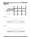
The PAGE PROGRAM instruction requires the following sequence. After the CE# line is pulled low to select the
device, the PAGE PROGRAM instruction is transmitted via the Sl line followed by the address and the data (D7-D0)
to be programmed (Refer to Table 7). Programming will start after the CE# pin is brought high. The low-to-high
transition of the CE# pin must occur during the SCK low time immediately after clocking in the D0 (LSB) data bit.
The READY/BUSY status of the device can be determined by initiating a RDSR instruction. If Bit 0 = 1, the program
cycle is still in progress. If Bit 0=0, the program cycle has ended. Only the RDSR instruction is enabled during the
program cycle. A single PROGRAM instruction programs 1 to 256 consecutive bytes within a page if it is not write
protected. The starting byte could be anywhere within the page. When the end of the page is reached, the address
will wrap around to the beginning of the same page. If the data to be programmed are less than a full page, the data
of all other bytes on the same page will remain unchanged. If more than 256 bytes of data are provided, the address
counter will roll over on the same page and the previous data provided will be replaced. The same byte cannot be
reprogrammed without erasing the whole sector/block first. The Pm25LV512/010 will automatically return to the
write disable state at the completion of the PROGRAM cycle.
Note: If the device is not write enabled (WREN) the device will ignore the Write instruction and will return to the
standby state, when CE# is brought high. A new CE# falling edge is required to re-initiate the serial
communication.
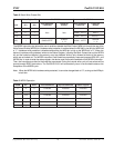
sserddA215VL52mP010VL52mP
A
N
A
51
A-
0
A
61
A-
0
stiBeraCt'noDA
32
A-
61
A
32
A-
71
Table 7. Address Key


