9
Programmable Microelectronics Corp. Issue Date: February, 2004, Rev: 1.4
PMC Pm25LV512/010
NEPWPWNEWskcolBdetcetorPskcolBdetcetorpnUretsigeRsutatS
0X 0 detcetorPdetcetorPdetcetorP
0X 1 detcetorPelbatirWelbatirW
1woL0 detcetorPdetcetorPdetcetorP
1woL1 detcetorPelbatirWdetcetorP
XhgiH0 detcetorPdetcetorPdetcetorP
XhgiH1 detcetorPelbatirWelbatirW
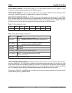
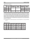
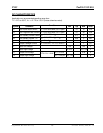
Table 6. WPEN Operation
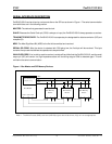
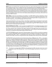
The WRSR instruction also allows the user to enable or disable the Write Protect (WP#) pin through the use of the
Write Protect Enable (WPEN) bit. Hardware write protection is enabled when the WP# pin is low and the WPEN bit
is "1". Hardware write protection is disabled when either the WP# pin is high or the WPEN bit is "0." When the
device is hardware write protected, writes to the Status Register, including the Block Protect bits and the WPEN
bit, and the locked-out blocks in the memory array are disabled. Write is only allowed to blocks of the memory
which are not locked out. The WRSR instruction is self-timed to automatically erase and program BP0, BP1, and
WPEN bits. In order to write the status register, the device must first be write enabled via the WREN instruction.
Then, the instruction and data for the three bits are entered. During the internal write cycle, all instructions will be
ignored except RDSR instructions. The Pm25LV512/010 will automatically return to write disable state at the
completion of the WRSR cycle.
Note: When the WPEN bit is hardware write protected, it cannot be changed back to "0", as long as the WP# pin
is held low.
leveL
stiBretsigeRsutatS215VL52mP010VL52mP
1PB0PB
sesserddAyarrA
tuOdekcoL
tuo-dekcoL
)s(kcolB
sesserddAyarrA
tuOdekcoL
tuo-dekcoL
)s(kcolB
000
enoNenoN
enoNenoN
)4/1(101 FFFF10-0008104kcolB
)2/1(210 FFFF10-0000104,3kcolB
)llA(311 FFFF00-000000
skcolBllA
)2-1(
FFFF10-000000
skcolBllA
)4-1(
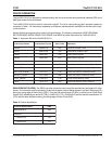
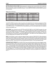
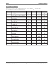
Table 5. Block Write Protect Bits


