


HD74LV2GT66A
Rev.2.00, Oct.17.2003, page 3 of 9
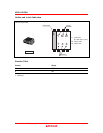
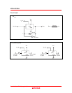
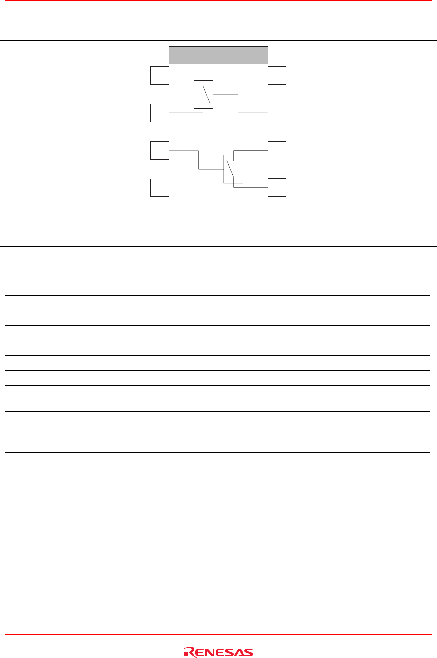
Pin Arrangement
(Top view)
8V
CC
1
7
CONT1
6
OUT / IN2
5
IN / OUT2
IN / OUT1
2
OUT / IN1
3
CONT2
4
GND
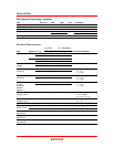
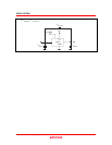
Absolute Maximum Ratings
Item Symbol Ratings Unit Test Conditions
Supply voltage range V
CC
–0.5 to 7.0 V
Input voltage range
*1
V
I
–0.5 to 7.0 V
Output voltage range
*1, 2
V
O
–0.5 to V
CC
+ 0.5 V Output : H or L
Input clamp current I
IK
–20 mA V
I
< 0
Output clamp current I
OK
±50 mA V
O
< 0 or V
O
> V
CC
Continuous output current I
O
±25 mA V
O
= 0 to V
CC
Continuous current through
V
CC
or GND
I
CC
or I
GND
±50 mA
Maximum power dissipation
at Ta = 25°C (in still air)
*3
P
T
200 mW
Storage temperature Tstg –65 to 150 °C
Notes: The absolute maximum ratings are values, which must not individually be exceeded, and
furthermore no two of which may be realized at the same time.
1. The input and output voltage ratings may be exceeded if the input and output clamp-current
ratings are observed.
2. This value is limited to 5.5 V maximum.
3. The maximum package power dissipation was calculated using a junction temperature of 150°C.