


( 27 / 38 )
5.8 Pulldown Transistor Control
Since ports D4 to D7, E0 and G0 to G3 contain emulation circuits, you can not control the pulldown
resistors using the pulldown control register. If you want to use the internal pulldown resistors, turn
on switches SW4 to SW10 when occasion demands. With the M34282T5-OPT, the port's resistance
value of the pulldown resistor is 150 kΩ.
When changing the resistance value of the pulldown resistor, replace RA1 (ports E0, G3 to G0) and
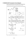
RA2 (ports G7 to G4) on the M34282T5-OPT. For the position of the pulldown resistor, see Figure 4.3.
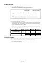
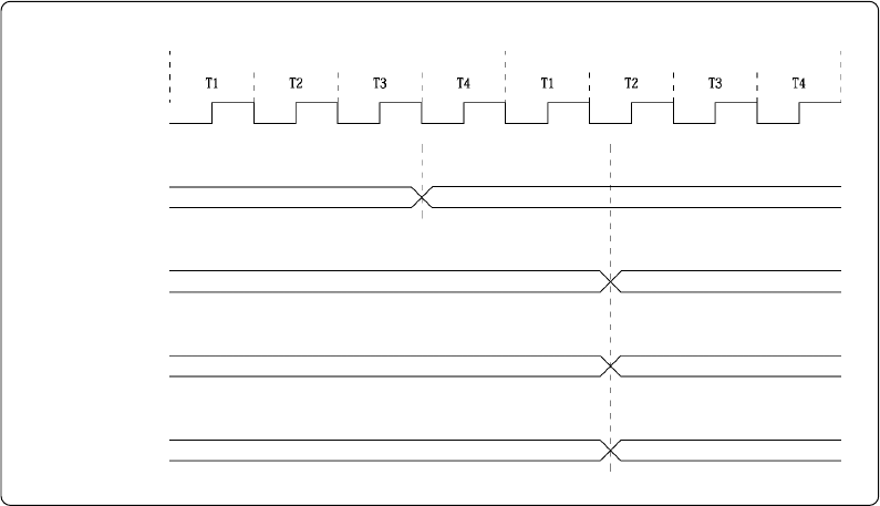
5.9 Port I/O Timing
(1) Port input timing
Port input timings are the same as with the actual MCUs.
(2) Port output timing
When using the M34282T5-OPT, output timings are different from those of the actual MCUs for
the ports D0 to D7, E0 and G0 to G3 that are configured with port emulation circuits.
With the actual MCUs, changes occur at the beginning of the T4 state of an output instruction.
With the M34282T5-OPT, changes occur at the beginning of the T2 state of the next output
instruction. Figure 5.2 shows the port timings of the actual MCUs and M34282T5-OPT.
Port output timings of ports E1, E2 and CARR are the same as with the actual MCUs.
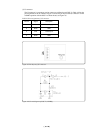
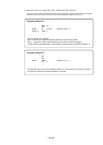
Figure 5.2 Ports D, E and G output timings
Output Instruction Next output Instruction
Instruction clock
STCK
Ports D, E and G
output timing
of actual MCU
Port D
output timing
of M34282T5-OPT
Port E
output timing
of M34282T5-OPT
Port G
output timing
of M34282T5-OPT