Functional Overview
2.8 Reset Module
Rev.1.00 June 1,2005 2-14
REJ11J0002-0100Z
2
2.8 Reset Module
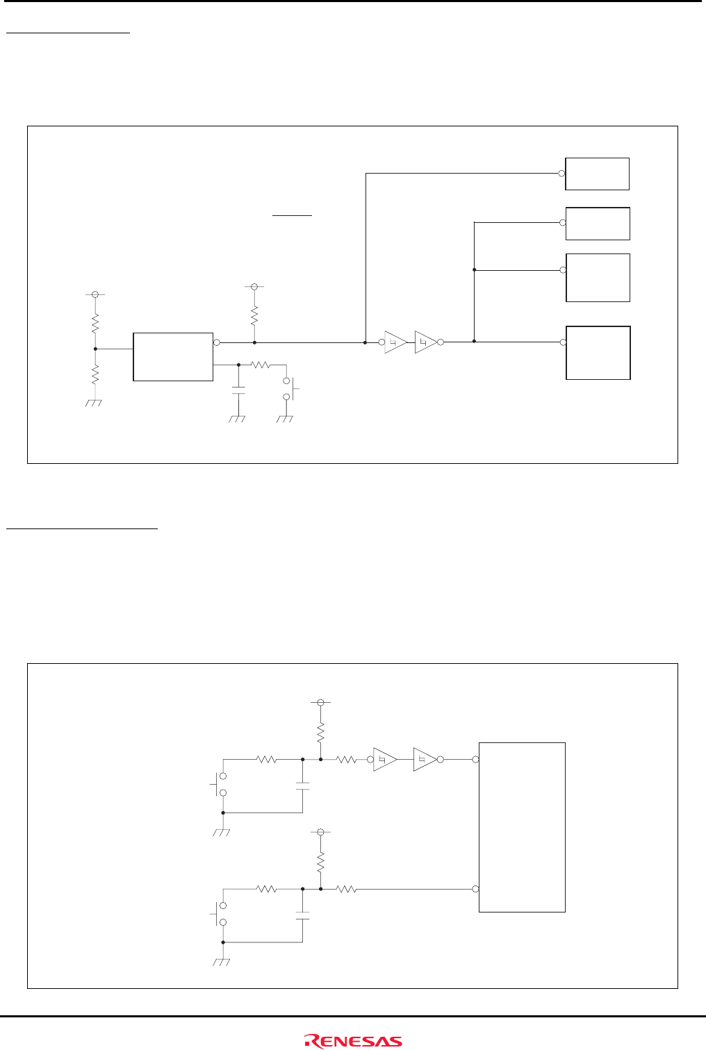
This module controls the reset signals connected to both the SH7206 and Flash memory mounted in the M3A-HS60.
Figure2.8.1 shows a block diagram of the reset module in M3A-HS60.
3.3V
Reset switch
SW 2
Reset IC
M51957BFP
Input
Delay capacitance
Flash memory
*
*
Open-collector output
Output
3.3V
RP#
Ra
Rb
Cd
R
esetIC output delay time,td=0.34 x Cd(pF)µsec = 34ms
R
esetIC output detection voltage,Vs = 1.25 x = 2.5V
)
Rb
Ra+Rb
)
10KW
10KW
0.1µF
Extension connect
or
RESET#
RES#
SH7206
H-UDI connector
RES#
Figure2.8.1 Block Diagram of Reset Module
2.9 Interrupt Switches
As for the M3A-HS60, both the SH7206's NMI interrupt pin and MRES pin have a push switch connected. MRES switch
can be used for controlling manual reset for SH7206. When manual reset is done, the internal condition of CPU will be
formatted, but each register of on-chip peripheral module.
Figure2.9.1 shows a block diagram of interrupt switches.
NMI switch
SH7206
3.3V
NMI#
SW 5
M
RES switch
3.3V
MRES#/PE13
SW 6
Figure2.9.1 Block Diagram of Interrupt Switches


