Operational Specifications
3.1.5 User I/O Connectors (J6-J8)
Rev.1.00 June 1,2005 3-7
REJ11J0002-0100Z
3
3.1.5 User I/O Connectors (J6-J8)
The through-hole for the extension connector pin connecting the pins of the on-chip peripheral functions (such as MTU2
and AD), which is suitable for the motor control of SH7206, is mounted on M3A-HS60.
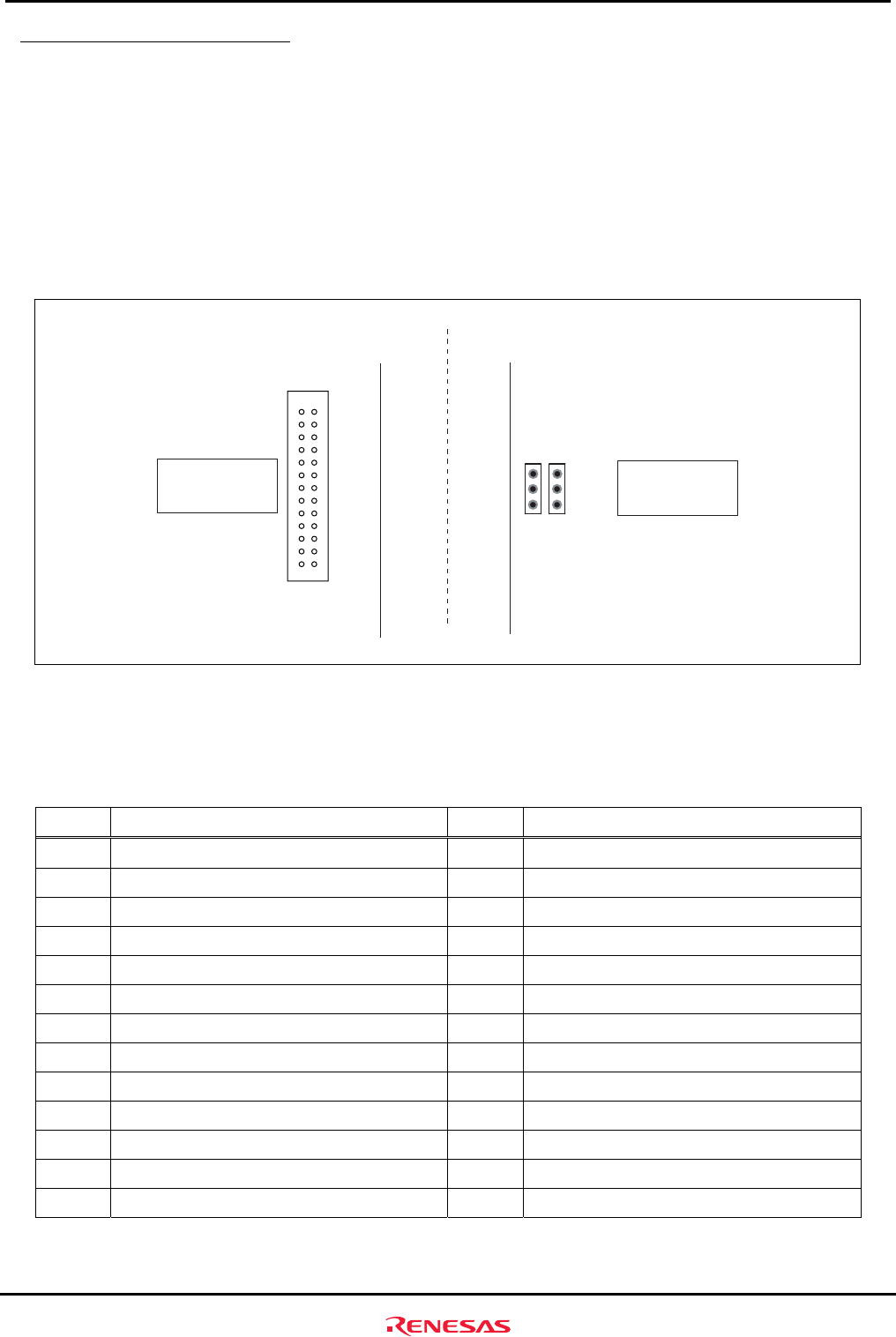
Figure3.1.6 shows a pin arrangement of extension connector.
Note: The J6 connects the pins multiplexed to data bus (D31-D16) of SH7206. Therefore, the data bus D31–D16
becomes unusable when the J6 is used. Please set the SDRAM bus width to 16-bit wide (D15-D0) when the J6 is being
used.
Board edge
1
2
3
J7 J8
Board edge
1
2
3
12
2526
Top view of the
Component side
Top view of the
Solder side
Figure3.1.6 Pin Assignment of Extension Connectors (J6-J8)
Table3.1.6 and Table3.1.7 list pin assignments of the extension connectors.
Table3.1.6 Pin Assignments of Extension Connector (J6)
Pin Signal Name Pin Signal Name
1
+5V
2
GND
3
NC (AN3/PF3 when R66 is mounted)
4
D27/DACK1/TIOC4AS/PD27
5
D26/DACK0/TIOC4BS/PD26
6
D25/DREQ1/TIOC4CS/PD25
7
SCK3/TIOC3B/RTS3#/PE9
8
TXD3/TIOC4A/PE12
9
MRES#/TIOC4B/PE13
10
RXD3/TIOC3D/CTS3#/PE11
11
DACK1/CKE/TIOC4D/IRQOUT#/PE15
12
WE3#/ICIOWR#/AH#/DACK0/TIOC4C/PE14
13
D20/IRQ4/TIC5WS/PD20
14
D21/IRQ5/TIC5VS/PD21
15
D22/IRQ6/TIC5US/AUDCK/PD22
16
D19/IRQ3/POE7#/AUDATA3/PD19
17
AN2/PF2
18
AN3/PF3
19
AN4/PF4
20
NC(AN4/PF4 when R67 is mounted)
21
D28/CS2#/TIOC3DS/PD28
22
D29/CS3#/TIOC3BS/PD29
23
D30/TIOC3CS/IRQOUT#/PD30
24
D31/TIOC3AS/ADTRG#/PD31
25
AN0/PF0
26
AN1/PF1


