


ELECTRICAL SPECIFICATION SSD-DXXX(I)-3600 DATA SHEET
SILICONSYSTEMS PROPRIETARY
This document and the information contained within it is confidential and proprietary to SiliconSystems, Inc.
All unauthorized use and/or reproduction is prohibited.
3600D-04DSR PAGE 12 FEBRUARY 2, 2009
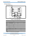
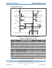
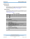
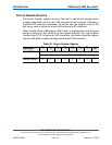
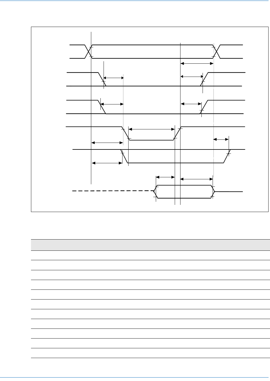
I/O Access Write Timing
Figure 5: I/O Access Write Timing Diagram
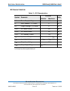
Note: (1) IOIS16 and INPACK are not supported.
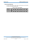
Table 13: I/O Access Write Timing
Symbol Parameter Minimum Maximum Units
t
IGHDX
Data Hold following IOWR 5 - ns
t
IGHQX
Data Setup before IOWR 20 - ns
t
IGLIGH
IOWR Pulse Width 65 - ns
t
AVIGL
Address Setup before IOWR 25 - ns
t
AXIGH
Address Hold following IOWR 10 - ns
t
CLIGL
CE Setup before IOWR 5 - ns
t
CHIGH
CE Hold following IOWR 10 - ns
t
RLIGL
REG Setup before IOWR 5 - ns
t
RHIGH
REG Hold following IOWR 0 - ns
t
AVISL
IOIS16 Delay Falling from Address - (1) ns
t
AXISH
IOIS16 Delay Rising from Address - (1) ns
A[10::0]
____
REG
__
CE
_____
IOWR
______
IOIS16
tRLIGL
tAXIGH
D[15::0]
tCLIGL
tCHI GH
tRHIGH
tIGLIGH
tAXISH
tAVISL
tAVIGL
tIGHQX
tIGHDX