


LIST OF TABLES SSD-DXXX(I)-3600 DATA SHEET
SILICONSYSTEMS PROPRIETARY
This document and the information contained within it is confidential and proprietary to SiliconSystems, Inc.
All unauthorized use and/or reproduction is prohibited.
3600D-04DSR PAGE VII FEBRUARY 2, 2009
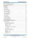
LIST OF TABLES
Table 1: System Performance ......................................................................................... 3
Table 2: System Power Requirements ............................................................................ 3
Table 3: Reliability............................................................................................................4
Table 4: Operational Life Span ........................................................................................ 4
Table 5: Product Capacity Specifications ........................................................................ 5
Table 6: Environmental Specifications............................................................................. 5
Table 7: Pin Assignments ................................................................................................ 6
Table 8: Signal Descriptions ............................................................................................ 7
Table 9: Absolute Maximum Ratings ............................................................................... 9
Table 10: Capacitance..................................................................................................... 9
Table 11: DC Characteristics......................................................................................... 10
Table 12: I/O Access Read Timing ................................................................................ 11
Table 13: I/O Access Write Timing ................................................................................ 12
Table 14: True IDE Read/Write Access Timing ............................................................. 13
Table 15: True IDE Multiword DMA Read/Write Access Timing.................................... 14
Table 16: Task File Register Specification..................................................................... 15
Table 17: Error Register................................................................................................. 16
Table 18: Feature Register ............................................................................................ 17
Table 19: Sector Count Register.................................................................................... 18
Table 20: Sector Number Register ................................................................................ 19
Table 21: Cylinder Low Register.................................................................................... 20
Table 22: Cylinder High Register................................................................................... 21
Table 23: Drive/Head Register....................................................................................... 22
Table 24: Status Register .............................................................................................. 23
Table 25: Command Register........................................................................................ 24
Table 26: Alternate Status Register............................................................................... 25
Table 27: Device Control Register................................................................................. 26