


Si53xx-RM
Rev. 0.5 37
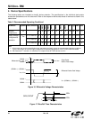
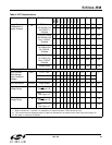
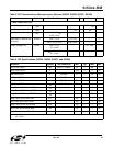
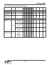
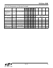
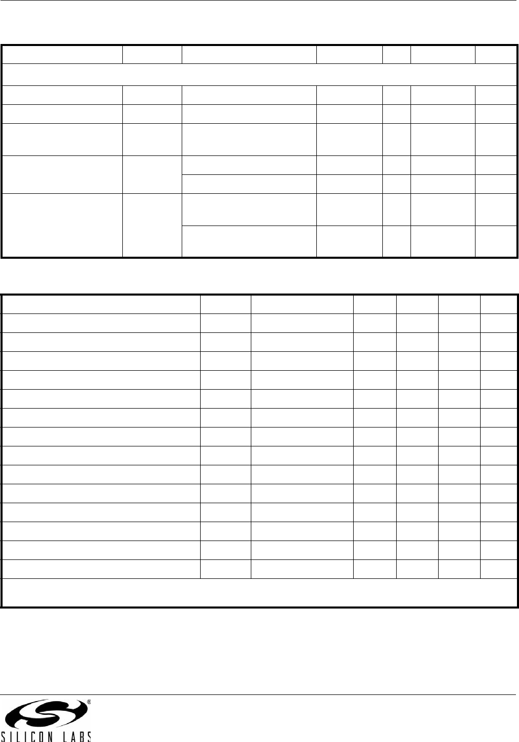
Table 5. DC Characteristics—Microprocessor Devices (Si5324, Si5325, Si5367, Si5368)
Parameter Symbol Test Condition Min Typ Max Units
I
2
C Bus Lines (SDA, SCL)
Input Voltage Low V
ILI2C
— — 0.25 x V
DD
V
Input Voltage High V
IHI2C
0.7 x V
DD
—V
DD
V
Input Current I
II2C
VIN = 0.1 x V
DD
to 0.9 x V
DD
–10 — 10 µA
Hysteresis of Schmitt trig-
ger inputs
V
HYSI2C
V
DD
= 1.8 V 0.1 x V
DD
—— V
V
DD
= 2.5 or 3.3 V 0.05 x V
DD
—— V
Output Voltage Low V
OHI2C
V
DD
=1.8V
IO = 3 mA
——0.2xV
DD
V
V
DD
= 2.5 or 3.3 V
IO = 3 mA
——0.4 V
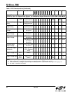
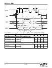
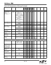
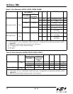
Table 6. SPI Specifications (Si5324, Si5325, Si5367, and Si5368)
Parameter Symbol Test Conditions Min Typ Max Unit
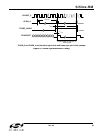
Duty Cycle, SCLK t
DC
SCLK = 10 MHz 40 — 60 %
Cycle Time, SCLK t
c
100 — — ns
Rise Time, SCLK t
r
20–80% — — 25 ns
Fall Time, SCLK t
f
20–80% — — 25 ns
Low Time, SCLK t
lsc
20–20% 30 — — ns
High Time, SCLK t
hsc
80–80% 30 — — ns
Delay Time, SCLK Fall to SDO Active t
d1
——25ns
Delay Time, SCLK Fall to SDO Transition t
d2
——25ns
Delay Time, SS Rise to SDO Tri-state t
d3
——25ns
Setup Time, SS to SCLK Fall t
su1
25 — — ns
Hold Time, SS to SCLK Rise t
h1
20 — — ns
Setup Time, SDI to SCLK Rise t
su2
25 — — ns
Hold Time, SDI to SCLK Rise t
h2
20 — — ns
Delay Time between Slave Selects t
cs
25 — — ns
Note: All timing is referenced to the 50% level of the waveform unless otherwise noted. Input test levels are VIH = V
DD
–4V,
VIL=0.4V.