


Si53xx-RM
Rev. 0.5 7
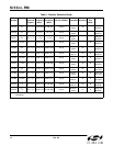
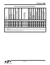
L IST OF FIGURES
Figure 1. Si5316 Any-Frequency Jitter Attenuator Block Diagram . . . . . . . . . . . . . . . . . . . . . 17
Figure 2. Si5319 Any-Frequency Jitter Attenuating Clock Multiplier Block Diagram . . . . . . . .18
Figure 3. Si5322 Low Jitter Clock Multiplier Block Diagram . . . . . . . . . . . . . . . . . . . . . . . . . . 19
Figure 4. Si5323 Jitter Attenuating Clock Multiplier Block Diagram . . . . . . . . . . . . . . . . . . . . 20
Figure 5. Si5324 Clock Multiplier and Jitter Attenuator Block Diagram. . . . . . . . . . . . . . . . . . 21
Figure 6. Si5325 Low Jitter Clock Multiplier Block Diagram . . . . . . . . . . . . . . . . . . . . . . . . . . 22
Figure 7. Si5326 Clock Multiplier and Jitter Attenuator Block Diagram. . . . . . . . . . . . . . . . . . 23
Figure 8. Si5327 Clock Multiplier and Jitter Attenuator Block Diagram. . . . . . . . . . . . . . . . . . 24
Figure 9. Si5365 Low Jitter Clock Multiplier Block Diagram . . . . . . . . . . . . . . . . . . . . . . . . . . 25
Figure 10. Si5366 Jitter Attenuating Clock Multiplier Block Diagram . . . . . . . . . . . . . . . . . . . 26
Figure 11. Si5367 Clock Multiplier Block Diagram . . . . . . . . . . . . . . . . . . . . . . . . . . . . . . . . . 27
Figure 12. Si5368 Clock Multiplier and Jitter Attenuator Block Diagram. . . . . . . . . . . . . . . . . 28
Figure 13. Si5369 Clock Multiplier and Jitter Attenuator Block Diagram. . . . . . . . . . . . . . . . . 29
Figure 14. Si5374 Functional Block Diagram . . . . . . . . . . . . . . . . . . . . . . . . . . . . . . . . . . . . . 30
Figure 15. Si5375 Functional Block Diagram . . . . . . . . . . . . . . . . . . . . . . . . . . . . . . . . . . . . . 31
Figure 16. Differential Voltage Characteristics . . . . . . . . . . . . . . . . . . . . . . . . . . . . . . . . . . . . 32
Figure 17. Rise/Fall Time Characteristics . . . . . . . . . . . . . . . . . . . . . . . . . . . . . . . . . . . . . . . . 32
Figure 18. SPI Timing Diagram . . . . . . . . . . . . . . . . . . . . . . . . . . . . . . . . . . . . . . . . . . . . . . . . 38
Figure 19. Frame Synchronization Timing . . . . . . . . . . . . . . . . . . . . . . . . . . . . . . . . . . . . . . . 39
Figure 20. Any-Frequency Precision Clock DSPLL Block Diagram . . . . . . . . . . . . . . . . . . . . 46
Figure 21. Clock Multiplication Circuit . . . . . . . . . . . . . . . . . . . . . . . . . . . . . . . . . . . . . . . . . . . 47
Figure 22. PLL Jitter Transfer Mask/Template . . . . . . . . . . . . . . . . . . . . . . . . . . . . . . . . . . . . 48
Figure 23. Jitter Tolerance Mask/Template. . . . . . . . . . . . . . . . . . . . . . . . . . . . . . . . . . . . . . . 49
Figure 24. Si5316 Divisor Ratios. . . . . . . . . . . . . . . . . . . . . . . . . . . . . . . . . . . . . . . . . . . . . . . 51
Figure 25. Wideband PLL Divider Settings (Si5325, Si5367) . . . . . . . . . . . . . . . . . . . . . . . . . 76
Figure 26. Narrowband PLL Divider Settings (Si5319, Si5324, Si5326,
Si5327, Si5368, Si5369, Si5374, Si5375) . . . . . . . . . . . . . . . . . . . . . . . . . . . . . . . 78
Figure
27. Si5324, Si5325, Si5326, Si5327, and Si5374 Input Clock Selection . . . . . . . . . . . 81
Figure 28. Si5367, Si5368, and Si5369 Input Clock Selection . . . . . . . . . . . . . . . . . . . . . . . . 82
Figure 29. Free Run Mode Block Diagram . . . . . . . . . . . . . . . . . . . . . . . . . . . . . . . . . . . . . . . . 85
Figure 30. Parameters in History Value of M . . . . . . . . . . . . . . . . . . . . . . . . . . . . . . . . . . . . . 87
Figure 31. Digital Hold vs. VCO Freeze Example . . . . . . . . . . . . . . . . . . . . . . . . . . . . . . . . . . 89
Figure 32. Frame Sync Frequencies . . . . . . . . . . . . . . . . . . . . . . . . . . . . . . . . . . . . . . . . . . . . 92
Figure 33. FOS Compare . . . . . . . . . . . . . . . . . . . . . . . . . . . . . . . . . . . . . . . . . . . . . . . . . . . . 98
Figure 34. I
2
C Command Format . . . . . . . . . . . . . . . . . . . . . . . . . . . . . . . . . . . . . . . . . . . . . 102
Figure 35. I2C Example. . . . . . . . . . . . . . . . . . . . . . . . . . . . . . . . . . . . . . . . . . . . . . . . . . . . . 102
Figure 36. SPI Write/Set Address Command . . . . . . . . . . . . . . . . . . . . . . . . . . . . . . . . . . . . 104
Figure 37. SPI Read Command . . . . . . . . . . . . . . . . . . . . . . . . . . . . . . . . . . . . . . . . . . . . . . 104
Figure 38. Differential LVPECL Termination . . . . . . . . . . . . . . . . . . . . . . . . . . . . . . . . . . . . . 105
Figure 39. Single-Ended LVPECL Termination. . . . . . . . . . . . . . . . . . . . . . . . . . . . . . . . . . . 105
Figure 40. CML/LVDS Termination (1.8, 2.5, 3.3 V) . . . . . . . . . . . . . . . . . . . . . . . . . . . . . . . 106
Figure 41. CMOS Termination (1.8, 2.5, 3.3 V). . . . . . . . . . . . . . . . . . . . . . . . . . . . . . . . . . . 106
Figure 42. Typical Output Circuit (Differential) . . . . . . . . . . . . . . . . . . . . . . . . . . . . . . . . . . . 107