


Si53xx-RM
76 Rev. 0.5
7. Microprocessor Controlled Parts (Si5319, Si5324, Si5325, Si5326, Si5327,
Si5367, Si5368, Si5369, Si5374, Si5375)
The devices in this family provide a rich set of clock multiplication/clock division options, loop bandwidth selections,
output clock phase adjustment, and device control options.
7.1. Clock Multiplication
The input frequency, clock multiplication ratio, and output frequency are set via register settings. Because the
DSPLL dividers settings are directly programmable, a wide range of frequency translations is available. In addition,
a wider range of frequency translations is available in narrowband parts than wideband parts due to the lower
phase detector frequency range in narrowband parts. To assist users in finding valid divider settings for a particular
input frequency and clock multiplication ratio, Silicon Laboratories offers the DSPLLsim utility to calculate these
settings automatically. When multiple divider combinations produce the same output frequency, the software
recommends the divider settings that yield the best combination of phase noise performance and power
consumption.
7.1.1. Jitter Tolerance (Si5319, Si5324, Si5325, Si5326, Si5327, Si5368, Si5369, Si5374 and Si5375)
See Section 5.2.3.
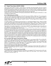
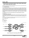
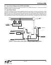
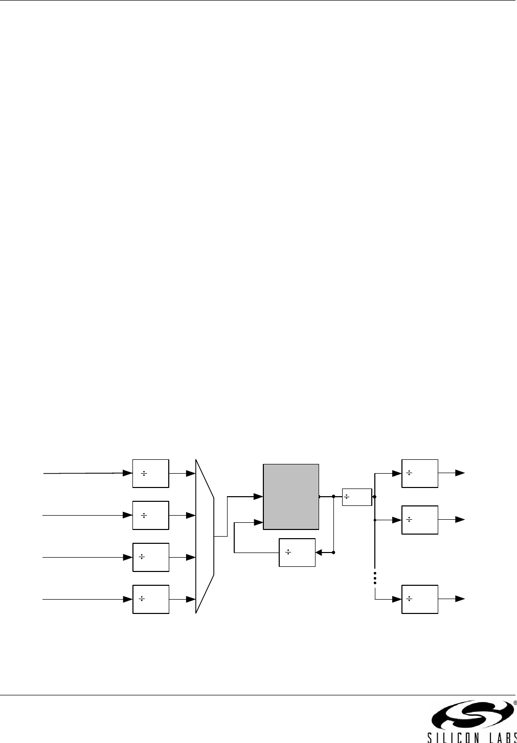
7.1.2. Wideband Parts (Si5325, Si5367)
These devices operate as wideband clock multipliers without an external resonator or reference clock. This mode
may be desirable if the input clock is already low jitter and only simple clock multiplication is required. A limited
selection of clock multiplication factors is available in this mode. The input-to-output skew for wideband parts is not
controlled.
Refer to Figure 25. The selected input clock passes through the N3 input divider and is provided to the DSPLL. The
input-to-output clock multiplication ratio is defined as follows:
f
OUT
= f
IN
x N2/(N1 x N3)
where:
N1 = output divider
N2 = feedback divider
N3 = input divider
Figure 25. Wideband PLL Divider Settings (Si5325, Si5367)
2
/
CKIN1
N31
/CKIN2 N32
2
2
N2
N2 = N2_LS
N2_LS = [32, 34, 36, …, 512]
NC1
NC2
/
CKOUT_1
/
CKOUT_2
2
4.85 – 5.67 GHz
f
IN
=
10 MHz–710 MHz
f
OUT
= 2 kHz -–1. 4 GHz
/
CKIN3
N33
/
CKIN4
N34
2
2
10 MHz–
157.5 MHz
NC1 = N1_ HS x N1_LS
N1_ HS = [4,5,6,...,11]
N1_ LS = [1,2,4,6,...,2
20
]
NC5
/
CKOUT_5
2
f
3
f
3
N1
N3 =
[1,2,3,...,2
19
]
f
OSC
DSPLL
®
N1_HS