


ARM720T_LH79520 – Sharp LH79520 SoC with ARM720T 32-bit RISC Processor
clock signal (CLK_I), an acknowledge signal fails to appear from the addressed slave peripheral device, the wait request to the
ARM720T is dropped, the processor times out normally and the current data transfer cycle is forcibly terminated.
The ACK_O signal from a slave peripheral should not be used as a ‘long delay’ hand-shaking mechanism. Where such a
mechanism needs to be implemented, either use polling or interrupts.
For more information on connection of slave physical memory and peripheral I/O devices to the processor's Wishbone
interfaces, refer to the application note
Connecting Memory and Peripheral Devices to a 32-bit Processor.
Data Organization
Data organization refers to the ordering of the data during transfers. There are two general types of ordering:
• BIG ENDIAN – the most significant portion of an operand is stored at the lower address
•
LITTLE ENDIAN – the most significant portion of an operand is stored at the higher address.
The ARM720T_LH79520 supports both of these, but is left in its default Little Endian mode after a reset. To use Big Endian data,
you would need to configure the processor accordingly. Refer to the
ARM720T Technical Reference Manual for further
information.
Words, Half-Words and Bytes
The ARM720T_LH79520 operates on the following data sizes:
• 32-bit words
• 16-bit half-words
• 8-bit bytes.
There are dedicated load and store instructions for these three data types.
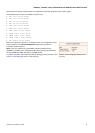
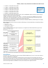
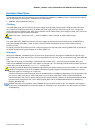
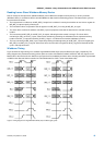
Figure 8 shows how these different sizes of data are organized relative to each other over an 8-byte memory range in the
ARM720T_LH79520.
Word-1 Word-0
31 24 23 16 15 8 7 0 31 24 23 16 15 8 7 0
Half-3 Half-2 Half-1 Half-0
15 8 7 0 15 8 7 0 15 8 7 0 15 8 7 0
Byte-7 Byte-6 Byte-5 Byte-4 Byte-3 Byte-2 Byte-1 Byte-0
7 0 7 0 7 0 7 0 7 0 7 0 7 0 7 0
Figure 8. Organization of data types for the ARM720T_LH79520 (Little Endian).
Physical Interface to Memory and Peripherals
The ARM720T_LH79520's physical interface to the outside world is always 32 bits wide. Since the addressing has a byte-level
resolution, this means that up to four "packets" of data (bytes) can be loaded or stored during a single memory access. To
accommodate this requirement all memory accesses (8-bit, 16-bit and 32-bit) are handled in a specific way.
Each 32-bit read and write can be considered as a read or write through four "byte-lanes". These byte-lanes are marked as valid
by the corresponding bits in the PER_WEB[3..0] and subsequent SEL_O[3..0] signal of the relevant Wishbone interface
(External Memory or Peripheral I/O). Each of these bits will be active if the byte data in that lane is valid. This allows a single
byte to be written to 32-bit wide memory without needing to use a slower read-modify-write cycle.
The instructions of the ARM720T_LH79520 require that all 32-bit load/store operations be aligned on 4-byte boundaries and all
16-bit load/store operations be aligned on 2-byte boundaries. Byte operations (8-bit) can be to any address.
To complete a byte load or store, the ARM720T_LH79520 will position the byte data in the correct byte-lane and set the
PER_WEB/SEL_O signal for that lane active. The memory hardware must then only enable writing on the relevant 8-bits of data
from the 32-bit word.
When reading, the ARM720T_LH79520 will put the relevant 8- or 16-bit value into the LSB's of the 32-bit word. What happens
with the remaining bits depends on the operation:
CR0162 (v2.0) March 10, 2008 15