


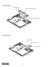
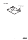
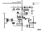
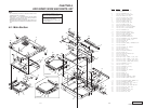

PCGA-DSD5/DSM5 (UC)
Confidential
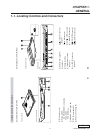
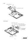
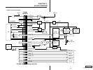
D_PWRSRC_ON*
DOCK_+VPWRSRC
D_+VDC_IN
PC_SENSE*
+VPWRSRC
DC/DC
Conv.
+VDC_IN
BATT+
D_PWRGD
D_INUSE
+VCC3
Reg.
USB I/F
i.LINK
PHY Chip
Floppy Disk
Drive
Hi-Side
Switch
USB_PWR_ON
Serial I/F
Parallel I/F
Docking
Connector
VGA
Ethernet
i.LINK
Bridge Chip
Optical Disc
Drive
ATAPIPHY-LINK
DOCKED*
DC IN
+VCC5
H8
RESET
IC
UNDOCK SW
i.LINK
Network SW
SUS_ON*
USB_EN
UNDOCK_SW*
Docking
Station
Indicator
D_INUSE
MPBID1ICH
PCG-R505 Side
Docking Station Side
i.LINK I/F
i.LINK I/F
D_SUSPEND
RSRV_ID
INUSE_LED
USB Atype
DSUB-25
DSUB-9
DSUB-15
RJ-45
i.LINK-4
x 2
BUS SW
FD I/F FD I/F
FDDBUS
4-1 4-2
CHAPTER 4.
BLOCK DIAGRAM
– OVERALL BLOCK DIAGRAM –
(END)