SY-6IZM/3
Quick Start Guide
8
Hardware
Installation
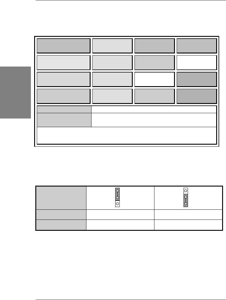
Step 3. Configure Memory
This Motherboard features 3 x DIMM for 168-pin 3.3V unbuffered DIMM
modules, providing support for up to 256MB of main memory using DIMM
modules from 8MB to 128MB.
Number of Memory
Modules
DIMM 1 DIMM 2 DIMM 3
1
Double-sided
/Single-sided
Double-sided
2
Double-sided
/Single-sided
Double-sided
3
Double-sided
/Single-sided
Single-sided Single-sided
RAM Type
SDRAM
Memory Module
Size (MB)
8/16/32/64/128 Mbytes
Note: Because DIMM 2 and 3 are shared, double-sided DIMMs can be used
in only one of the DIMMs. With single-sided DIMMs both 2 and 3 can be used.
Step 4. Set JP3 for power up FSB clock and AGP bus clock.
JP3 is used to adjust AGP bus clock frequency depending on the value of the front side bus
(FSB) clock, also the setting of the JP3 determines the power up FSB clock which will
remain effective until the BIOS set the FSB clock to the CMOS setting.
JP3 Setting
Power up FSB Clock 66MHz 100MHz
AGP Clock
AGP Clock = FSB Clock ÷ 1 AGP Clock = FSB Clock ÷ 1.5
Note: The specification of maximum AGP bus Clock frequency is 66.6MHz.
∗
Set JP3 to pin 1-2 short when you use a FSB 100MHz CPU.
∗
Set JP3 to pin 2-3 short when you use a FSB 66MHz CPU.
∗
Set JP3 to pin 1-2 short when you use a FSB 66MHz CPU but want to over clock the
FSB clock to 100MHz via the BIOS setting.
2
1
3
2
1
3


