SY-7VCA Quick Start Guide
10
Hardware
Installation
Debug LEDs
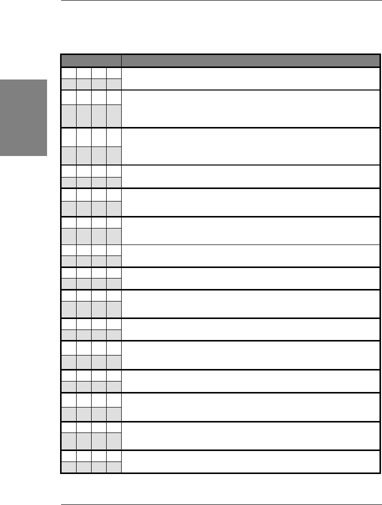
The Debug LEDs give an indication of the status of the system during boot-up. If the system
does not boot-up properly, use the table below to find out at what point in boot-up sequence
the problem arises. A x means the LED is off, a L means the LED is lit.
Code Explanation
X X X
L
D8 D3 D2 D1
Initialization of the chipset. The MCH and ICH registers will be set to the most
conservative values by the BIOS to make sure the system boots up properly.
X X L X
D8 D3 D2 D1
The BIOS is now decompressing the BIOS code into shadow RAM. Most of
the BIOS code is stored in the BIOS Flash ROM IC in compressed form to
save space. At boot-up this code is decompressed and stored to RAM for faster
execution.
X X L L
D8 D3 D2 D1
The checksum for the decompressed code is calculated and checked. The
checksum is calculated by adding all data bytes together and storing the result
in the BIOS ROM. If the calculated checksum is different from the checksum
stored in the ROM, the code stored in the FLASH ROM is corrupted.
X L X X
D8 D3 D2 D1
The chipset (MCH and ICH) registers are set to the values selected by the user.
X L X L
D8 D3 D2 D1
Now the BIOS will set the CPU Vcore voltage and the FSB bus frequency to
the user selected value. If the system stops at this point, the settings selected by
the user are inappropriate. Please select more conservative settings.
X L L X
D8 D3 D2 D1
The Hardware Monitor Functionality is initialized. The settings the user
selected in the BIOS for the Hardware Monitor are written into the Hardware
Monitor registers.
X L L L
D8 D3 D2 D1
If the VGA card does not work or is not inserted at all, the system will display
this code for a short period of time.
L X X X
D8 D3 D2 D1
At this point the BIOS is initializing the CPU. The L2 cache latency values are
set, and more important, the CPU micro-code is written into the CPU.
L X X L
D8 D3 D2 D1
Now the system is testing the RAM inserted on the board. The screen will
show the BIOS testing the RAM by a running counter. After finishing the test,
the screen will show the amount of RAM in your system.
L X L X
D8 D3 D2 D1
The super I/O registers are set to the default values. This includes the serial,
parallel and IR etc settings.
L X L L
D8 D3 D2 D1
At this point the IDE busses (primary and secondary) are scanned for devices.
This includes HD drives and ATAPI CD-ROM drives that are connected to the
IDE bus. After scanning the detected devices are displayed on screen.
L L X X
D8 D3 D2 D1
The serial and parallel port registers are set to the values selected by the user.
L L X L
D8 D3 D2 D1
Now the BIOS will scan the peripheral busses for add-on cards. This includes
the PCI and AGP busses. If any add-on cards are detected, the resources it
requires are assigned by the BIOS in accordance with user settings.
L L L X
D8 D3 D2 D1
The ESCD and DMI (Desktop Management Interface) values are checked. If
there are changes, the BIOS will flash the new values into the BIOS Flash
ROM IC.
L L L L
D8 D3 D2 D1
At this point the BIOS passes control to the Operating System (OS). All LEDs
will be on and will stay on to indicate a successful boot.


