


MII/RMII 10/100 Ethernet Transceiver with HP Auto-MDIX and flexPWR
®
Technology in a Small Footprint
Datasheet
SMSC LAN8710/LAN8710i 15 Revision 1.0 (04-15-09)
DATASHEET
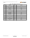
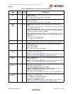
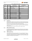
TXD2 24 I8 Transmit Data 2: The MAC transmits data to the transceiver using this
signal in MII Mode.
This signal should be grounded in RMII Mode.
TXD3 25 I8 Transmit Data 3: The MAC transmits data to the transceiver using this
signal in MII Mode.
This signal should be grounded in RMII Mode.
nINT/
TXER/
TXD4
18 IOPU nINT – Active low interrupt output. Place an external resistor pull-up to
VDDIO.
See Section 4.10 for information on how nINTSEL is used to determine
the function for this pin.
TXER – MII Transmit Error: When driven high, the 4B/5B encode process
substitutes the Transmit Error code-group (/H/) for the encoded data word.
This input is ignored in 10Base-T operation.
TXD4 – MII Transmit Data 4: In Symbol Interface (5B Decoding) mode, this
signal becomes the MII Transmit Data 4 line, the MSB of the 5-bit symbol
code-group.
TXD4 is not used in RMII Mode.
This signal is mux’d with nINT
TXEN 21 IPD Transmit Enable: Indicates that valid data is presented on the TXD[3:0]
signals, for transmission. In RMII Mode, only TXD[1:0] have valid data.
TXCLK 20 O8 Transmit Clock: Used to latch data from the MAC into the transceiver.
MII (100BT): 25MHz
MII (10BT): 2.5MHz
This signal is not used in RMII Mode.
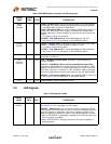
RXD0/
MODE0
11 IOPU RXD0 – Receive Data 0: Bit 0 of the 4 data bits that are sent by the
transceiver in the receive path.
MODE0 – PHY Operating Mode Bit 0: set the default MODE of the PHY.
See Section 5.3.9.2 for information on the MODE options.
RXD1/
MODE1
10 IOPU RXD1 – Receive Data 1: Bit 1 of the 4 data bits that are sent by the PHY
in the receive path.
MODE1 – PHY Operating Mode Bit 1: set the default MODE of the PHY.
See Section 5.3.9.2 for information on the MODE options.
RXD2/
RMIISEL
9IOPDRXD2 – Receive Data 2: Bit 2 of the 4 data bits that are sent by the
transceiver in the receive path.
The RXD2 signal is not used in RMII Mode.
RMIISEL – MII/RMII Mode Selection: Latched on the rising edge of the
internal reset (nRESET) based on the following strapping:
By default, MII mode is selected.
Pull this pin high to VDDIO with an external resistor to select RMII mode,
RXD3/
PHYAD2
8IOPDRXD3 – Receive Data 3: Bit 3 of the 4 data bits that are sent by the
transceiver in the receive path.
This signal is not used in RMII Mode.
This signal is mux’d with PHYAD2
PHYAD2 – PHY Address Bit 2: set the SMI address of the transceiver.
See Section 5.3.9.1 for information on the ADDRESS options.
Table 3.2 MII/RMII Signals (continued) 32-QFN (continued)
SIGNAL
NAME
32-QFN
PIN # TYPE DESCRIPTION