MII/RMII 10/100 Ethernet Transceiver with HP Auto-MDIX and flexPWR
®
Technology in a Small Footprint
Datasheet
Revision 1.0 (04-15-09) 16 SMSC LAN8710/LAN8710i
DATASHEET
3.2 LED Signals
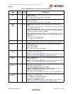
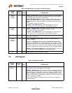
RXER/
RXD4/
PHYAD0
13 IOPD RXER – Receive Error: Asserted to indicate that an error was detected
somewhere in the frame presently being transferred from the transceiver.
The RXER signal is optional in RMII Mode.
RXD4 – MII Receive Data 4: In Symbol Interface (5B Decoding) mode, this
signal is the MII Receive Data 4 signal, the MSB of the received 5-bit
symbol code-group. Unless configured in this mode, the pin functions as
RXER.
This signal is mux’d with PHYAD0
PHYAD0 – PHY Address Bit 0: set the SMI address of the PHY.
See Section 5.3.9.1 for information on the ADDRESS options.
RXCLK/
PHYAD1
7IOPDRXCLK – Receive Clock: In MII mode, this pin is the receive clock output.
25MHz in 100Base-TX mode. 2.5MHz in 10Base-T mode.
This signal is mux’d with PHYAD1
PHYAD1 – PHY Address Bit 1: set the SMI address of the transceiver.
See Section 5.3.9.1 for information on the ADDRESS options.
RXDV 26 O8 Receive Data Valid: Indicates that recovered and decoded data is being
presented on RXD pins.
COL/
CRS_DV/
MODE2
15 IOPU COL – MII Mode Collision Detect: Asserted to indicate detection of
collision condition.
CRS_DV – RMII Mode CRS_DV (Carrier Sense/Receive Data Valid)
Asserted to indicate when the receive medium is non-idle. When a 10BT
packet is received, CRS_DV is asserted, but RXD[1:0] is held low until the
SFD byte (10101011) is received. In 10BT, half-duplex mode, transmitted
data is not looped back onto the receive data pins, per the RMII standard.
MODE2 – PHY Operating Mode Bit 2: set the default MODE of the PHY.
See Section 5.3.9.2 for information on the MODE options.
CRS 14 IOPD Carrier Sense: Indicates detection of carrier.
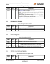
Table 3.3 LED Signals 32-QFN
SIGNAL
NAME
32-QFN
PIN # TYPE DESCRIPTION
LED1/
REGOFF
3IOPDLED1 – Link activity LED Indication.
See Section 5.3.7 for a description of LED modes.
REGOFF – Regulator Off: This pin may be used to configure the internal
1.2V regulator off. As described in Section 4.9, this pin is sampled during the
power-on sequence to determine if the internal regulator should turn on.
When the regulator is disabled, external 1.2V must be supplied to VDDCR.
When LED1/REGOFF is pulled high to VDD2A with an external resistor, the
internal regulator is disabled.
When LED1/REGOFF is floating or pulled low, the internal regulator is
enabled (default).
Table 3.2 MII/RMII Signals (continued) 32-QFN (continued)
SIGNAL
NAME
32-QFN
PIN # TYPE DESCRIPTION


