


ARCNET 5 Port HUB Controller
Datasheet
SMSC TMC2005-JT Page 21 Revision 1.1 (07-24-07)
DATASHEET
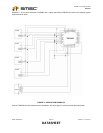
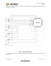
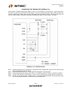
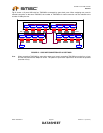
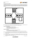
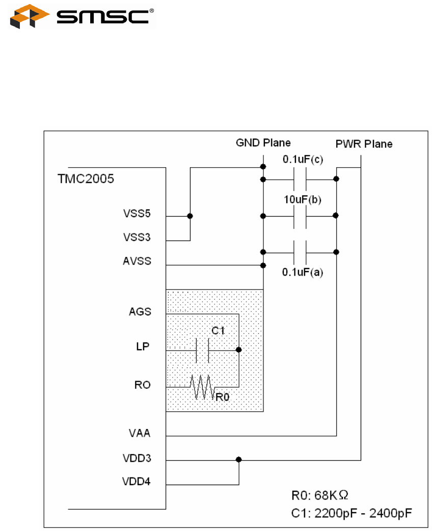
CONNECTING THE TMC2005 WITH INTERNAL PLL
When using the TMC2005 at data rate 2.5Mbps or lower, it is not necessary to use internal PLL. Leave the loop filter
pins (RO, LP) open and connect AGS to the Ground. The pins for the analog power supply (AVSS, AVDD) may
connect to digital power supply. When using the TMC2005 at data rate 5Mbps or higher, the internal PLL has to be
used as a clock multiplier. PCB layout must follow the guidelines at Figure 10, refer to Notes 1 through 5.
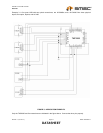
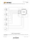
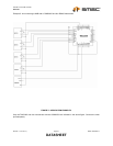
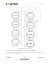
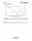
FIGURE 10 - PLL PATTERN LAYOUT
Note 1: Prohibit the patterns for LP and RO from occupying the area of digital power supply. Use the area of analog
power supply between VAA and AVSS.
Note 2: Encircle the pattern between LP, RO and AGS with wide pattern of analog ground.
Note 3: Connect the analog power supply “VAA” with 0.1 uF condenser (a) with in 1/8 inch (~ 3.2mm) from VAA pin.
Note 4: In order to filter the jitter of low frequency, connect a 10 uF condenser (b) in parallel with the condenser (a).
Note 5: Place 0.1 uF bypass condenser (c) within ¼ inch (~ 6.4mm) from VDD3 and VSS3. Connect the ground side
of a condenser (c) at the place (*) where AVSS returns to GND plane.