


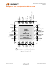
Integrated USB 2.0 Compatible 3-Port Hub
Datasheet
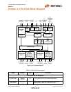
Revision 2.3 (08-27-07) 12 SMSC USB2503/USB2503A
DATASHEET
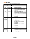
Crystal Output XTAL2 OCLKx 24MHz Crystal
This is the other terminal of the crystal, or left
unconnected when an external clock source is used to
drive XTAL1/CLKIN. It must not be used to drive any
external circuitry other than the crystal circuit.
Clock Input
Enable
CLKIN_EN I Clock In Enable:
Low = XTAL1 and XTAL2 pins configured for use with
external crystal
High = XTAL1 pin configured as CLKIN, and must be
driven by an external CMOS clock.
RESET Input RESET_N IS This active low signal is used by the system to reset the
chip. The minimum active low pulse is 100ns.
Self-Power /
Bus-Power
Detect
SELF_PWR I Detects availability of local self-power source.
Low = Self/local power source is NOT available (i.e., 7-
Port Hub gets all power from Upstream USB VBus).
High = Self/local power source is available.
TEST Pins TEST[1:0] IPD Used for testing the chip. User must treat as a no-
connect or connect to ground. For board testing, all
signal pins are included in an XNOR chain, Please see
Chapter 6, "XNOR Test," on page 37 for more details on
the configuration and use of the XNOR mode.
Analog Test
&
Internal 1.8V
voltage
regulator
enable
ATEST/
REG_EN
AIO This signal is used for testing the analog section of the
chip, and to enable or disable the internal 1.8v regulator.
This pin must be connected to VDDA3P3 to enable the
internal 1.8V regulator, or to VSS to disable the internal
regulator.
When the internal regulator is enabled, the 1.8V power
pins must be left unconnected, except for the required
bypass capacitors.When the PHY is in test mode, the
internal regulator is disabled and the ATEST pin
functions as a test pin.
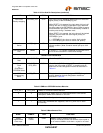
Table 4.4 Power, Ground, and No Connect
NAME SYMBOL TYPE FUNCTION
VDD1P8 VDD18 +1.8V core power.
If the internal regulator is enabled, then VDD18 pin
closest to VDD33CR must have a 4.7
μF (or greater)
±20% (ESR <0.1
Ω) capacitor to VSS
VDDPLL1P8 VDDA18PLL +1.8V Filtered analog power for internal PLL.
If the internal regulator is enabled, then this pin must
have a 4.7
μF (or greater) ±20% (ESR <0.1Ω) capacitor
to VSS
VDDAPLL3P3 VDDA33PLL +3.3V Filtered analog power for the internal PLL
If the internal PLL 1.8V regulator is enabled, then this pin
acts as the regulator input
VDDA3P3 VDDA33 +3.3V Filtered analog power.
Table 4.3 Miscellaneous Pins (continued)
NAME SYMBOL TYPE FUNCTION