


USB 2.0 Hi-Speed Hub Controller
Datasheet
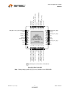
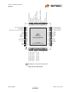
Revision 1.0 (3-11-09) 12 SMSC USB251x
DATASHEET
Chapter 5 Pin Descriptions
This chapter is organized by a set of pin configurations (organized by package type) followed by a
corresponding pin list organized alphabetically. A comprehensive and detailed description list of each
signal (named in the pin list) is organized by function in Table 5.2, “USB251x Pin Descriptions,” on
page 22. Please refer to Table 5.3, “Buffer Type Descriptions,” on page 27 for a list of buffer types.
The “N” symbol in the signal name indicates that the active, or asserted, state occurs when the signal
is at a low voltage level. When “N” is not present after the signal name, the signal is asserted when it
is at the high voltage level. The terms assertion and negation are used exclusively. This is done to
avoid confusion when working with a mixture of “active low” and “active high” signals. The term assert,
or assertion, indicates that a signal is active, independent of whether that level is represented by a
high or low voltage. The term negate, or negation, indicates that a signal is inactive.
5.1 Pin Configurations and Lists (Organized by Package Type)
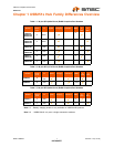
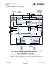
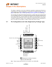
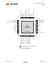
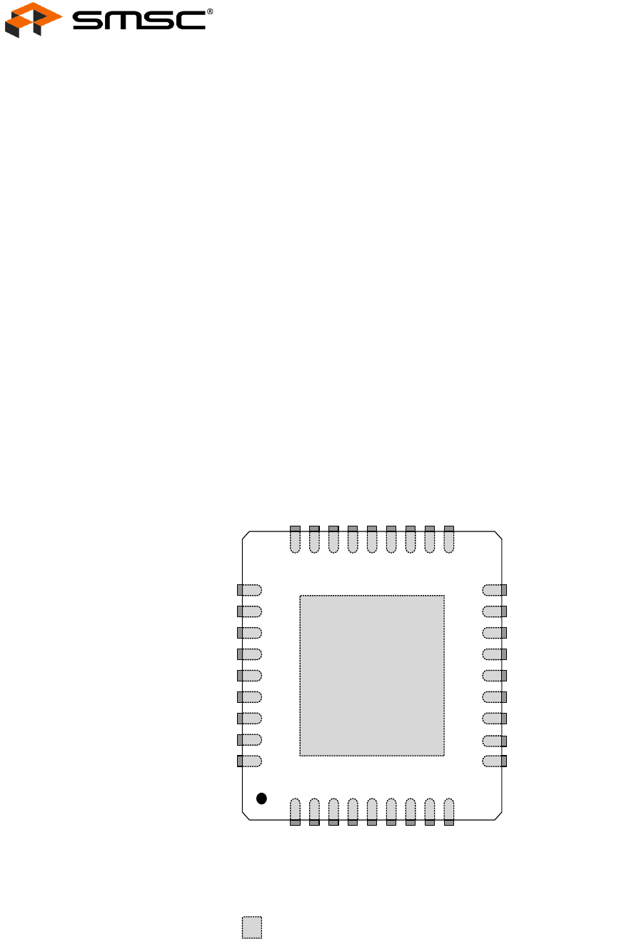
Figure 5.1 2-Port 36-Pin QFN
Note: *Battery charging enable (BC_EN) is only available in the USB251xB/Bi.
Ground Pad
(must be connected to VSS)
SMSC
USB2512/12A/12B
USB2512i/12Ai/12Bi
(Top View QFN-36)
26
VDD33
25
RESET_N
24
HS_IND / CFG_SEL[1]
23
SCL / SMBCLK / CFG_SEL[0]
22
SDA / SMBDATA / NON_REM[1]
21
NC
20
NC
19
VBUS_DET
27
NC
18
NC
17
OCS_N[2]
16
PRTPWR[2] / BC_EN[2]*
15
OCS_N[1]
14
VDD33
13
CRFILT
12
PRTPWR[1] / BC_EN[1]*
11
TEST
10
VDD33
SUSP_IND / LOCAL_PWR / NON_REM[0]
28
VDD33
29
USBDP_UP
31
XTALOUT
32
XTALIN / CLKIN
33
RBIAS
36
VDD33
35
PLLFILT
34
USBDM_UP
30
VDD33
1
USBDM_DN[1]
2
USBDP_DN[1]
3
USBDM_DN[2]
4
USBDP_DN[2]
5
NC
6
NC
7
NC
8
NC
9
Indicates pins on the bottom of the device.