


www.ti.com
0 5 10 15 20 25 30 35 40 45 50 55 60 65 70 75 80 85
f − Frequency − MHz
Amplitude − dBFS
G002
1
−135
−120
10
−130
−110
−100
−90
−80
−70
−60
−50
−40
−30
−20
−10
0
2
3
4
5
x
3.2.4ClockInput
3.2.5DigitalOutputs
CircuitDescription
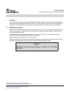
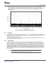
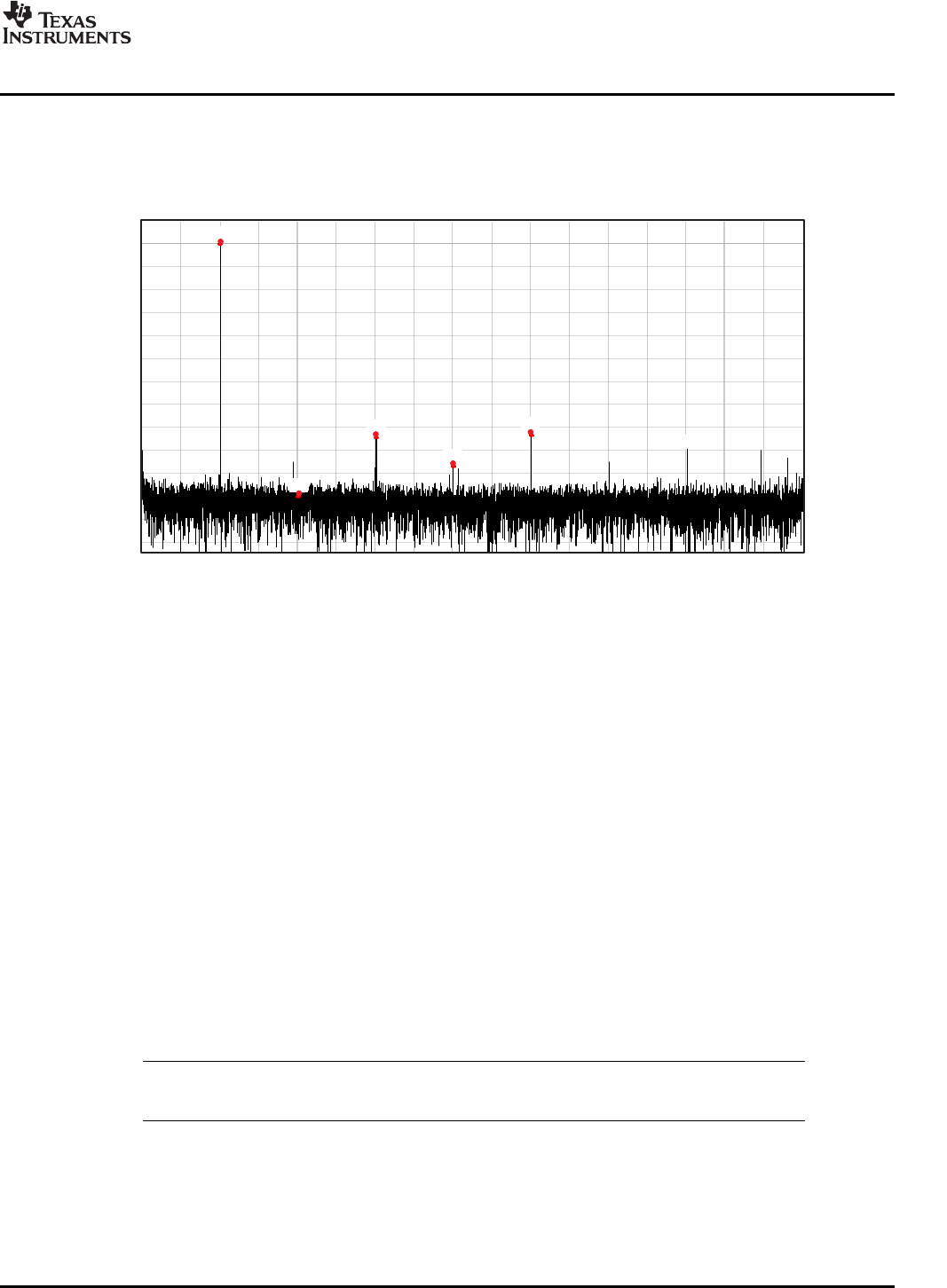
TheschematicspresentvariousinterfaceoptionsbetweentheamplifierandtheADC.Dependingon
theinputfrequenciesofinterest,furtherperformanceoptimizationcanbehadbydesigninga
correspondingfilter.Initsdefaultconfiguration,R43,R44,andC119formafirst-order,low-passfilter
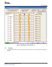
withacutofffrequencyof70MHz.Figure2showstheperformanceoftheADS5545usingthe
THS4509path.
Figure2.THS4509+ADS5545EVMPerformance
Asingle-ended,harmonicallyfiltered,low-phase-noise,1.5-VrmssinusoidalinputshouldbeappliedtoJ7.
Thefrequencymustnotexceedthedevicespecification.IntheEVMdefaultconfiguration,bothSPJ1and
SJP2musthavepins1and2shorted.
Intheboarddefaultconfiguration,thetransformerprovidessingle-endedtodifferentialconversion.The
transformerhasanimpedanceratioof4.
Forcompatibilitywithabroadrangeoflogicanalyzers,theEVMoutputs3.3-VparallelCMOSdataon
headerJ4,independentoftheADCoperationalmode.TheXilinx™Spartan™-3EFPGAprovidesthe
necessarytranslation,anditconfiguresitselfusingoneoftwodifferentlogicfilesstoredinthePROM,
basedontheEVMconfiguration.TheCMOSdataoutputoftheFPGAiscontainedindataheaderJ4and
isastandard40-pinheaderona100-milgrid,whichallowseasyconnectiontoalogicanalyzer.The
connectorpinoutislistedinTable3.Forquicksetup,theeyediagramisshowninFigure3.Nosetupor
hold-timeadjustmentsmustbemadetothelogicanalyzerifusingtherisingedgeoftheoutputclockto
latchinthedata.
Note:TheeyediagramshownistheoutputoftheFPGAat210MSPS,notthatoftheADC.For
theADCoutputtiming,seetherespectivedevicedatasheet.
SLWU028B–January2006–RevisedNovember20069
SubmitDocumentationFeedback