2-1
Chapter 2
2 Setup and Required Equipment
Both the SN65LVDS125A and the SN65LVDS250 LVDS driver output
characteristics are compliant with the requirements of the TIA/EIA-644
standard. LVDS drivers nominally provide a 350-mV differential signal, with
a 1.2-V offset from ground. These levels are attained when driving a 100-Ω
differential line-termination test load. This requirement includes the effects
of up to 32 standard receivers with their ground references offset up to ±1 V
from that of the driver. This common-mode loading limitation of LVDS
drivers affects how the driver’s characteristics are observed with this EVM,
and the test setup that follows in this manual.
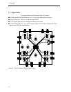
By using three power jacks (J17, J18, and J19) and by optionally installing
termination resistors, different methods of probing can be used to evaluate
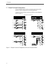
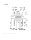
the device output characteristics. The typical setup for the 4x4 crosspoint
switch EVM is shown in Figure 2-1.
2.1 Applying an Input
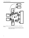
While the use of a split power plane allows the EVM to be terminated within
the oscilloscope, offsetting the EVM ground requires the inputs to the
device to also be offset. Figure 2-1 shows how to offset the EVM and the
inputs to the device. Setting power supply 1 to 3.3 V and power supply 2 to
1.2 V causes the voltage swing of the LVDS outputs to be within the limits
of -200 mV to 200 mV instead of the typical 1 V to 1.4 V. This requires the
inputs of the 4x4 crosspoint switch EVM to also be offset by 1.2 V, resulting
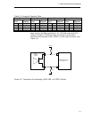
in a voltage swing of -200 mV to 200 mV. VTERM, banana jack J20, is
provided for non-LVDS input terminations such as LVPECL, which requires
a termination voltage. When applying an LVDS input, VTERM can be left
open or connected to GND, which is the common-mode voltage when using
the aforementioned –200-mV to 200-mV input swing.


