


Analog Input
5-2
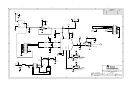
5.1 Analog Input
The analog input source can be applied directly to J1 (top or bottom side) or
through optional amplifier and signal conditioning modules. The analog input
range is dependent on the configuration of the EVM and the ADC installed at
location U1. Consult the datasheet for the device to determine the maximum
analog input range.
5.2 Digital Control
The digital control signals can be applied directly to J2 (top or bottom side).
The modular MSOP8 EVM can also be connected directly to a DSP or a micro
controller interface board, such as the HPA449. See the product folder for the
EVM or the installed device for a current list of compatible interface and/or
accessory boards.
5.3 Chip Select (Shut Down)
Jumper JMP2 is provided to allow the selection of the signals applied to the
chip select (/CS) or shutdown (SHDN) pin of the ADC installed on the EVM.
The factory default condition for the EVM is to place a shunt jumper between
pins 1-2 of JMP2. This allows the Frame Sync (FS) signal from DSP host
systems to be used as a chip select for the ADC. This signal originates from
J2.7. When JMP2 is moved to pins 2-3, the /CS (SHDN) signal is applied via
J2.1.
5.4 Digital I/O Buffers
Single gate buffers U3, U5 and U6 are provided to ensure the safe operation
of the modular MSOP8 EVM with low voltage host controllers. The digital I/O
voltage applied to these buffers via JMP3 should be set in accordance with the
operating voltage of the host controller.
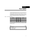
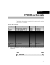
5.5 Default Jumper Locations
Table 5-1 provides a list of jumpers found on the EVM and their factory default
conditions.
Table 5-1.List of Jumpers
Jumper Shunt Position Jumper Description
JMP1 Pins 1-2 Controls ADC Supply Voltage (default is +5Va Source)
JMP2 Pins 1-2 Controls ADC /CS(SHDN) Pin (default is FS from DSP Host)
JMP3 Pins 5-6 Controls Digital I/O Voltage (default is +3.3Vd Source)
JMP4 CLOSED Ties ANALOG and DIGITAL grounds together
JMP5 Pins 1-2 Controls External Ref. Source (default is +2.5V from U2)
JMP6 Pins 1-2 Controls REFERENCE Source to ADC (default is onboard reference/buffer
circuit)