


SLUU130A – September 2002 – Revised February 2003
9
TPS40003-Based 5-A Converter in Less Than One Square Inch
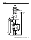
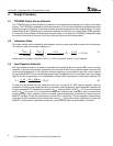
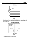
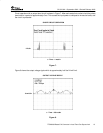
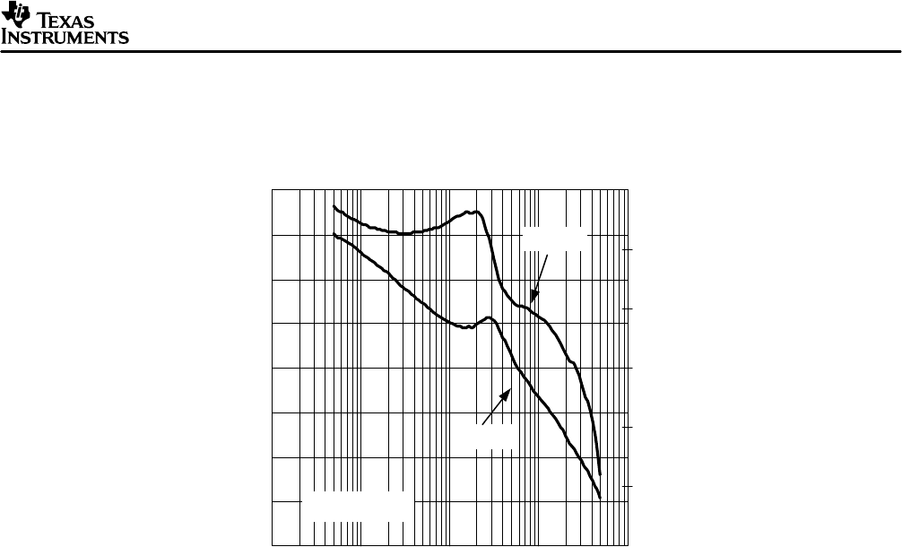
Figure 2 shows the plots for the closed loop gain and phase with V
IN
= 3.3 V and I
OUT
= 4.4 A. At the crossover
frequency of 60 kHz the phase margin is approximately 51 degrees.
100
150
100
50
0
–50
–100
40
30
20
10
0
–10
–20
–30
–40
1000 10000 1000000
Frequency – Hz
100000
Phase
–150
Gain – db
GAIN AND PHASE MARGIN
vs
FREQUENCY
Phase – degrees
I
LOAD
= 4.4 A
V
I
= 3.3 V
Gain
Figure 2.
4.8 Snubber Component Selection
The switch node where Q1 and L1 come together is very noisy. An R–C network fitted between this node and
ground can help reduce ringing and voltage overshoot on Q1:B. This ringing noise should be minimized to
prevent it from confusing the control circuitry which is monitoring this node for current limit and Predictive Gate
Drive.
As a starting point, the snubber capacitor, C9, is generally chosen to be 5 to 8 times larger than the parasitic
capacitance at the node, which is primarily C
OS
of Q1:B. Since C
OS
is 440 pF for Q1:B, C9 is chosen to be 3.3 nF.
R3 is empirically determined to be 2.2 Ω, which minimizes the ringing and overshoot at the switch node. With
low input voltages the power loss, 1/2×C×V
2
×f , is relatively small at 24 mW.