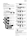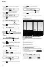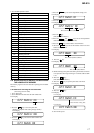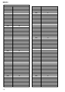
26
MZ-E10
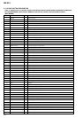
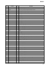
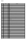
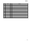
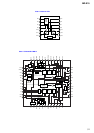
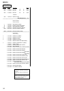
1 MWEB – Not used (open)
2 XD_MUTE O Mute signal output to Headphone
3 SIO4 DO O Serial data output to DC-DC convertor (SC901580EPR2)
4 (SIO4 DI) I Not used (Connected to ground)
5 SIO2 CLK O Serial clock output to EEPROM
6 NV XCS O Chip select signal output to EEPROM
7 SIO2 DO O Serial data output to EEPROM
8 SIO2 DI I Serial data input from EEPROM
9AVSS – Ground
10 UNREG MON I UNREG voltage monitor input
11 RF VCMON I Reference voltage (VC) input from RF AMP (SN761058ZQL)
12 RMC KEY1 I Remoto control key signal input
13 CHG_VI_MON I AC adapter voltage input
14 RF_TMP_MON I signal monitor input
15 OPEN CLS SW I Cassette lid open/close signal input
16 SET KEY I Key signal input
17 CHG MON I Battery charge ∆V detect and charge current monitor input
18 AVDD – Power supply
19 RMC DTCK I/O Serial data input/output
20 (RMC SPCK) – Not used (open)
21 SBUS CLK O Serial clock output to RF AMP (SN761058ZQL)
22 SBUS DATA I/O Serial data input/output to RF AMP (SN761058ZQL)
23 PWR_CLK_PWM O Clock output to DC-DC converter (SC901580EPR2)
24 AMICE CLK PWM O PWM signal output to RF AMP (SN761058ZQL)
25 DSP INTB – Not used (open)
26 DSP WRQB – Not used (open)
27 DRV FG INT – Not used (open)
28 DRV SLEDI INT – Not used (open)
29 XCHG I LIMIT O Limit charge current control signal
30 OPR_LED_O_CTL O LED (orange) control signal output
31 (LOCAL CHK1) – Not used (open)
32 CHG AD SEL O Monitor control of charge A/D signal
33 VCC2 – Power supply
34 VSS – Ground
35 PWR FFCLR O Latch and clear signal output to DC/DC converter (SC91580EPR2)
36 PWR SLEEP O Sleep signal output to DC/DC converter (SC91580EPR2)
37 PWR STRB O Strobe signal output to DC/DC converter (SC91580EPR2)
38 CHG AMP SEL O Select signal output of charge control
39 CHG PWM O Charge control PWM signal output
40 D_VO_PWM O Power supply control PWM signal output of Headphone AMP (NJU8713V-TE2)
41 OPR LED G PWM O LED (green) control signal output
42 OPR LED R PWM O LED (red) control signal output
43 VDD – Power supply
44 VSS – Ground
45 D_EN1 O Drive control signal output to Headphone AMP (NJU-8713V-TE2)
46 PD S1 O PD-IC mode select signal output to optical pick-up
47 XRF_RESET O Reset signal output to RF AMP (SN761058ZQL)
48 (LOCAL CHK2) – Not used (open)
49 SMON4 – Not used (open)
DescriptionPin Name
Pin No.
I/O
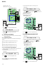
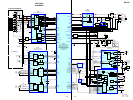
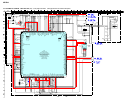
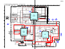
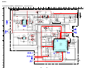
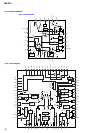
• IC601 LC-896442-VH4-16-E (DIGITAL SIGNAL PROCESSOR, DIGITAL SERVO SIGNAL PROCESSOR, EFM/ACIRC
ENCODER/DECODER, SHOCK PROOF MEMORY CONTROLLER, 16M BIT D-RAM, SYSTEM CONTROL)
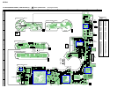
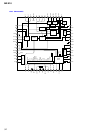
(MAIN BOARD)
6-7. IC PIN FUNCTION DESCRINTION