


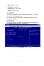
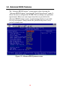
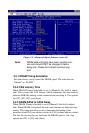
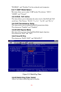
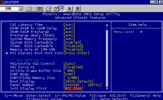
Figure 3.5: Advanced
chipset features screen (b)
Note:
DRAM default timings have
been carefully cho-
sen and should ONLY
be changed
if data is
being lost.
Please first contact technical
sup-
port.
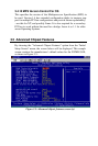
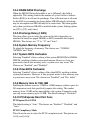
3.5.1 DRAM Timing Selectable
This item
allows
you to control
the
DRAM speed.
The selections are
“Manual”
or “By SPD”.
3.5.2 CAS Latency Time
When DRAM
Timing Selectable is set
to [Manual], this
field
is adjust-
able. This
controls the
CAS latency,
which
determines the time interval
between SDRAM starting
a read command and
receiving it. The
options
are
[3T], [4T], [5T], and
[Auto].
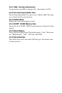
3.5.3 DRAM RAS# to CAS# Delay
When DRAM
Timing selectable
is set to [Manual], this
field
is adjust-
able.
When DRAM is
refreshed, the
rows and columns
are addressed
sep-
arately.
This setup
item allows user to
determine the
timing of
the
transition
from RAS (row address strobe)
to
CAS (column address strobe).
The less the clock
cycles are, the faster the DRAM
speed
is. Set- ting
options are [2T]
to
[5T], and [Auto].