


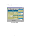
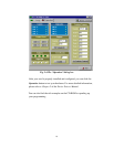


21
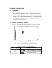
3.3 Signal Connections
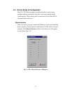
Pin Assignment
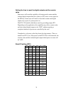
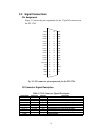
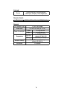
Figure 3-2 shows the pin assignments for the 37-pin I/O connector on
the PCI-1784.
EGND 1 20 CH0A-
CH0A+ 2 21 CH0B-
CH0B+ 3 22 CH0Z-
CH0Z+ 4 23 CH1A-
CH1A+ 5 24 CH1B-
CH1B+ 6 25 CH1Z-
CH1Z+ 7 26 CH2A-
CH2A+ 8 27 CH2B-
CH2B+ 9 28 CH2Z-
CH2Z+ 10 29 CH3A-
CH3A+ 11 30 CH3B-
CH3B+ 12 31 CH3Z-
CH3Z+ 13 32 EGND
IDI COM 14 33 IDI1
IDI0 15 34 IDI3
IDI2 16 35 EGND
EGND 17 36 IDO1
IDO0 18 37 IDO3
IDO2 19
.
Fig. 3-2 I/O connector pin assignments for the PCI-1784
I/O Connector Signal Description
Table 3-2 I/O Connector Signal Description
Signal Name Reference Direction Description
EGND - - External Ground.
CH<0..3>A+ EGND Input Channel <0..3> A differential positive-input.
CH<0..3>A- EGND Input Channel <0..3> A differential negative-input.
CH<0..3>B+ EGND Input Channel <0..3> B differential positive-input.
CH<0..3>B- EGND Input Channel <0..3> B differential negative-input.
CH<0..3>Z+ EGND Input Channel <0..3> Z differential positive-input.
CH<0..3>Z- EGND Input Channel <0..3> Z differential negative-input.
IDI<0..3> IDI COM Input Isolated Digital Input, Channels 0 through 3.
IDI COM - - Common input of the Isolated Digital Input.
IDO<0..3> EGND Output Isolated Digital Output, Channels 0 through 3.
EGND - - External Ground.