


PCI-6872 User’s Manual 24
Chapter 3 Software Configuration
3.1 Introduction
The system BIOS and custom drivers are located in a
256 KB, 32-pin (JEDEC spec.) Flash ROM device, designated U10. A
single Flash chip holds the system BIOS, VGA BIOS, and network Boot
ROM image. The display can be configured via software. This method
minimizes the number of chips and eases configuration. You can change
the display BIOS simply by reprogramming the Flash chip.
3.2 VGA display firmware configuration
The board’s on-board VGA interface supports a wide range of popular
LCD, EL, gas plasma flat panel displays and traditional analog CRT mon-
itors. The optimized shared memory architecture supports an 8/16/32 MB
frame buffer using system memory to provide resolutions of 1280 x 1024
@ 16 bpp, the interface can drive CRT displays with resolutions up to
1024 x 768 @ 16 bpp and 800 x 600 @ 16 bpp.
The VGA interface is configured completely via the software utility, so
you do not have to set any jumpers. Configure the VGA display as fol-
lows:
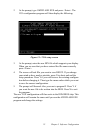
1. Apply power to the board with a color TFT display attached. This
is the default setting for this board. Ensure that the AWD-
FLASH.EXE and *.BIN files are located in the working drive.
NOTE: Ensure that you do not run AWDFLASH.EXE
while your system is operating in EMM386
mode.