PCM-9588 User Manual 44
! Test Write Multiple Output Pins
– Click the radio button- Multiple-Pins.
– Key in the pin number from ‘0x01’ to ‘0x0F’ to choose the multiple pin num-
bers to write the value of the output pin. The pin numbers are ordered bit-
wise, i.e. bit 0 stands for GPIO 0, bit 1 stands for GPIO 1, etc. For example, if
you want to write pin 0, 1, and 3, the pin numbers should be ‘0x0B’.
– Key in the value in (R/W) Result field from ‘0x01’ to ‘0x0F’ to write the value
of the output pin. The pin numbers are ordered bitwise, i.e. bit 0 stands for
GPIO 0, bit 1 stands for GPIO 1, etc. For example, if you want to set pin 0
and 1 high, 3 to low, the pin number should be ‘0x0B’, and then you should
key in the value ‘0x0A’ to write.
– Click the WRITE GPIO DATA button to write the GPIO output pins.
4.3.4.5 I
2
C
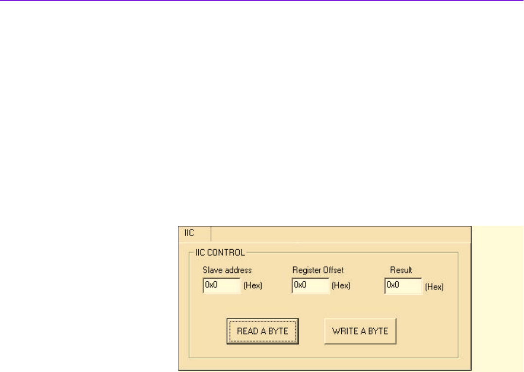
When the application is executed, you can read or write a byte of data through I
2
C
devices. All data must be read or written in hexadecimal system.
! Read a byte
– Key in the slave device address in Slave address field.
– Key in the register offset in Register Offset field.
– Click the READ A BYTE button and then a byte of data from the device will
be shown on the Result field.
! Write a byte
– Key in the slave device address in Slave address field.
– Key in the register offset in Register Offset field.
– Key in the desirous of data in Result field to write to the device.
– Click the WRITE A BYTE button and then the data will be written to the
device through I
2
C.


