Your ePlatform Partner
User’s Manual for Advantech SOM-A2552 series module V1.00
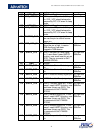
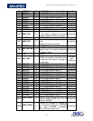
28
B28
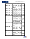
ADDR19 O SoC PXA255 system address 19 No pulling
A28
ADDR21 O SoC PXA255 system address 21 No pulling
B29
ADDR23 O SoC PXA255 system address 23 No pulling
A29
DATA0 IO SoC PXA255 system data 0 No pulling
B30
DATA1 IO SoC PXA255 system data 1 No pulling
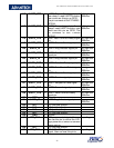
A30
DATA2 IO SoC PXA255 system data 2 No pulling
B31
DATA3 IO SoC PXA255 system data 3 No pulling
A31
DATA4 IO SoC PXA255 system data 4 No pulling
B32
DATA5 IO SoC PXA255 system data 5 No pulling
A32
DATA6 IO SoC PXA255 system data 6 No pulling
B33
DATA7 IO SoC PXA255 system data 7 No pulling
A33
DATA16 IO SoC PXA255 system data 16 No pulling
B34
DATA17 IO SoC PXA255 system data 17 No pulling
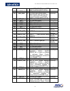
A34
DATA18 IO SoC PXA255 system data 18 No pulling
B35
DATA19 IO SoC PXA255 system data 19 No pulling
A35
DATA20 IO SoC PXA255 system data 20 No pulling
B36
DATA21 IO SoC PXA255 system data 21 No pulling
A36
DATA22 IO SoC PXA255 system data 22 No pulling
B37
DATA23 IO SoC PXA255 system data 23 No pulling
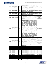
A37
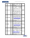
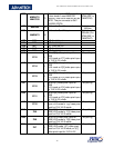
nBUF_SDCA
S
O
SDRAM CAS.
Connect to the
column address strobe (CAS) pins
for all banks of SDRAM.
No pulling
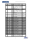
B38
nBUF_SDCS
2
O
SDRAM CS for banks 2. Connect to
the chip select (CS) pins for SDRAM.
For the PXA255 processor nSDCS0
can be Hi-Z, Nsdcs1-3 cannot.
No pulling
A38
BUF_DQM1 O
SDRAM DQM for data bytes 1.
Connect to the data output mask
enables (DQM) for SDRAM.
No pulling
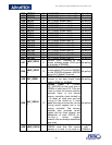
B39
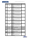
BUF_SDCLK
2
O
SDRAM Clock 2.
Connect
BUF_SDCLK[2] to the clock pins of
SDRAM in bank pairs 2/3. They are
driven
by either the internal memory
controller clock, or the internal
memory controller clock divided by
2. At reset, all clock pins are free
running at the divide by 2 clock
speed and may be turned off via free
running control register bits in the
memory contr
oller. The memory
controller also provides control
register bits for clock division and
deassertion of each SDCLK pin.
SDCLK[2:1] control register
assertion bits are always deasserted
upon reset.
No pulling
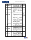
A39
nBUF_IOIS16
I
IO Select 16. Acknowledge from
the
PCMCIA card that the current
address is a valid 16 bit wide I/O
Pull high
with
100Kohm


