


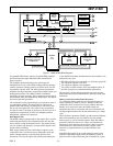
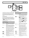
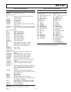
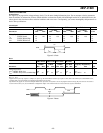

FUNCTIONAL BLOCK DIAGRAM
EXTERNAL
ADDRESS
BUSES
PROGRAM
SEQUENCER
EXTERNAL
DATA
BUSES
DATA ADDRESS
GENERATORS
DAG 1 DAG 2
PROGRAM MEMORY ADDRESS
PROGRAM MEMORY DATA
DATA MEMORY DATA
DATA MEMORY ADDRESS
INSTRUCTION
CACHE
ARITHMETIC UNITS
SHIFTERMULTIPLIER
ALU
REGISTER FILE
TIMER
JTAG TEST
& EMULATION
REV. C
Information furnished by Analog Devices is believed to be accurate and
reliable. However, no responsibility is assumed by Analog Devices for its
use, nor for any infringements of patents or other rights of third parties
which may result from its use. No license is granted by implication or
otherwise under any patent or patent rights of Analog Devices.
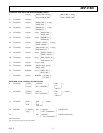
a
32/40-Bit IEEE Floating-Point
DSP Microprocessor
ADSP-21020
One Technology Way, P.O. Box 9106, Norwood, MA 02062-9106, U.S.A.
Tel: 617/329-4700 Fax: 617/326-8703
GENERAL DESCRIPTION
The ADSP-21020 is the first member of Analog Devices’ family
of single-chip IEEE floating-point processors optimized for
digital signal processing applications. Its architecture is similar
to that of Analog Devices’ ADSP-2100 family of fixed-point
DSP processors.
Fabricated in a high-speed, low-power CMOS process, the
ADSP-21020 has a 30 ns instruction cycle time. With a high-
performance on-chip instruction cache, the ADSP-21020 can
execute every instruction in a single cycle.
The ADSP-21020 features:
•
Independent Parallel Computation Units
The arithmetic/logic unit (ALU), multiplier and shifter
perform single-cycle instructions. The units are architecturally
arranged in parallel, maximizing computational throughput. A
single multifunction instruction executes parallel ALU and
FEATURES
Superscalar IEEE Floating-Point Processor
Off-Chip Harvard Architecture Maximizes Signal
Processing Performance
30 ns, 33.3 MIPS Instruction Rate, Single-Cycle
Execution
100 MFLOPS Peak, 66 MFLOPS Sustained Performance
1024-Point Complex FFT Benchmark: 0.58 ms
Divide (y/x): 180 ns
Inverse Square Root (1/√
x): 270 ns
32-Bit Single-Precision and 40-Bit Extended-Precision
IEEE Floating-Point Data Formats
32-Bit Fixed-Point Formats, Integer and Fractional,
with 80-Bit Accumulators
IEEE Exception Handling with Interrupt on Exception
Three Independent Computation Units: Multiplier,
ALU, and Barrel Shifter
Dual Data Address Generators with Indirect, Immedi-
ate, Modulo, and Bit Reverse Addressing Modes
Two Off-Chip Memory Transfers in Parallel with
Instruction Fetch and Single-Cycle Multiply & ALU
Operations
Multiply with Add & Subtract for FFT Butterfly
Computation
Efficient Program Sequencing with Zero-Overhead
Looping: Single-Cycle Loop Setup
Single-Cycle Register File Context Switch
15 (or 25) ns External RAM Access Time for Zero-Wait-
State, 30 (or 40) ns Instruction Execution
IEEE JTAG Standard 1149.1 Test Access Port and
On-Chip Emulation Circuitry
223-Pin PGA Package (Ceramic)
multiplier operations. These computation units support IEEE
32-bit single-precision floating-point, extended precision
40-bit floating-point, and 32-bit fixed-point data formats.
•
Data Register File
A general-purpose data register file is used for transferring
data between the computation units and the data buses, and
for storing intermediate results. This 10-port (16-register)
register file, combined with the ADSP-21020’s Harvard
architecture, allows unconstrained data flow between
computation units and off-chip memory.
•
Single-Cycle Fetch of Instruction and Two Operands
The ADSP-21020 uses a modified Harvard architecture in
which data memory stores data and program memory stores
both instructions and data. Because of its separate program
and data memory buses and on-chip instruction cache, the
processor can simultaneously fetch an operand from data
memory, an operand from program memory, and an
instruction from the cache, all in a single cycle.
•
Memory Interface
Addressing of external memory devices by the ADSP-21020 is
facilitated by on-chip decoding of high-order address lines to
generate memory bank select signals. Separate control lines
are also generated for simplified addressing of page-mode
DRAM.
The ADSP-21020 provides programmable memory wait
states, and external memory acknowledge controls allow
interfacing to peripheral devices with variable access times.